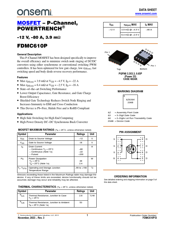
Datasheet4U Logo Datasheet4U.com

FDMC610P - P-Channel MOSFET

Datasheet Summary

Description

This P

the overall efficiency and to minimize switch node ringing of DC/DC converters using either synchronous or conventional switching PWM controllers.

Features

  • Max rDS(on) = 3.9 mW at VGS =.
  • 4.5 V, ID =.
  • 22 A.
  • Max rDS(on) = 6.4 mW at VGS =.
  • 2.5 V, ID =.
  • 16 A.
  • State.
  • of.
  • the.
  • art Switching Performance.
  • Lower Output Capacitance, Gate Resistance, and Gate Charge Boost Efficiency.
  • Shielded Gate Technology Reduces Switch Node Ringing and Increases Immunity to EMI and Cross Conduction.
  • This Device is Pb.
  • Free, Halide Free and is RoHS Compliant A.

📥 Download Datasheet

Datasheet preview – FDMC610P

Datasheet Details

Part number FDMC610P
Manufacturer ON Semiconductor
File Size 369.32 KB
Description P-Channel MOSFET
Datasheet download datasheet FDMC610P Datasheet
Additional preview pages of the FDMC610P datasheet.
Other Datasheets by ON Semiconductor

Full PDF Text Transcription

Click to expand full text
MOSFET – P-Channel, POWERTRENCH) -12 V, -80 A, 3.9 mW FDMC610P General Description This P−Channel MOSFET has been designed specifically to improve the overall efficiency and to minimize switch node ringing of DC/DC converters using either synchronous or conventional switching PWM controllers. It has been optimized for low gate charge, low rDS(on), fast switching speed and body diode reverse recovery performance. Features • Max rDS(on) = 3.9 mW at VGS = −4.5 V, ID = −22 A • Max rDS(on) = 6.4 mW at VGS = −2.
Published: |