FDC6331L Overview
Key Specifications
Package: SOP
Mount Type: Surface Mount
Pins: 6
Operating Voltage: 6.4 V
Description
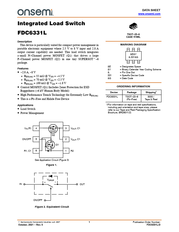
This device is particularly suited for compact power management in portable electronic equipment where 2.5 V to 8 V input and 2.8 A output current capability are needed. This load switch integrates a small N-Channel power MOSFET (Q1) that drives a large P-Channel power MOSFET (Q2) in one tiny SUPERSOTt-6 package.
Key Features
- RDS(on) = 55 mW @ VGS = -4.5 V
- RDS(on) = 70 mW @ VGS = -2.5 V
- RDS(on) = 100 mW @ VGS = -1.8 V
- Control MOSFET (Q1) Includes Zener Protection for ESD Ruggedness (>6 kV Human Body Model)
- High Performance Trench Technology for Extremely Low RDS(on)