PHK04P02T
PHK04P02T is P-channel vertical D-MOS logic level FET manufactured by NXP Semiconductors.
P-channel vertical D-MOS logic level FET
Rev. 02
- 14 December 2010 Product data sheet
1. Product profile
1.1 General description
Logic level P-channel enhancement mode Field-Effect Transistor (FET) in a plastic package using vertical D-MOS technology. This product is designed and qualified for use in puting, munications, consumer and industrial applications only.
1.2 Features and benefits
- Suitable for high frequency applications due to fast switching characteristics
- Suitable for logic level gate drive sources
- Suitable for very low gate drive sources voltage
1.3 Applications
- Battery powered applications
- High-speed digital interfaces
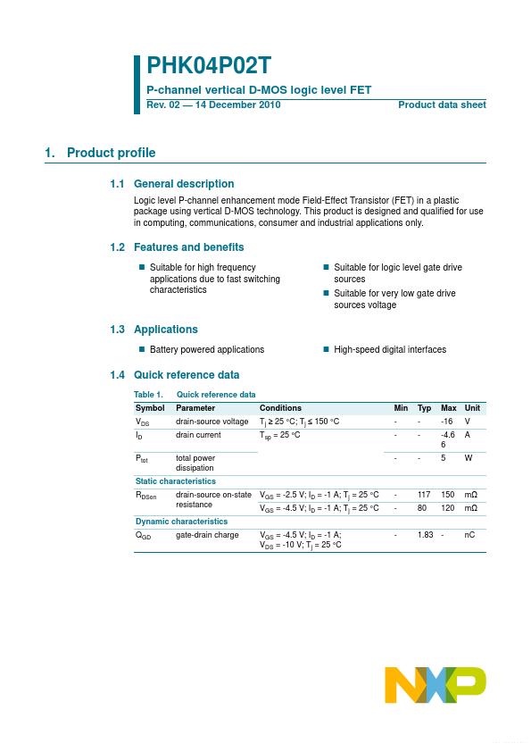
1.4 Quick reference data
Table 1. Symbol VDS ID Ptot Quick reference data Parameter drain-source voltage drain current total power dissipation drain-source on-state resistance VGS = -2.5 V; ID = -1 A; Tj = 25 °C VGS = -4.5 V; ID = -1 A; Tj = 25 °C VGS = -4.5 V; ID = -1 A; VDS = -10 V; Tj = 25 °C Conditions Tj ≥ 25 °C; Tj ≤ 150 °C Tsp = 25 °C Min Typ Max Unit -16 -4.6 6 5 V A W
Static characteristics RDSon 117 80 150 120 mΩ mΩ n C
Dynamic characteristics QGD gate-drain charge 1.83
- F r e e
D a t a s h e e t
NXP Semiconductors
P-channel vertical D-MOS logic level FET
2. Pinning information
Table 2. Pin 1 2 3 4 5 6 7 8 Pinning information Symbol Description S S S G D D D D source source source gate drain drain drain drain
1 4 S
001aaa025
Simplified outline
8 5
Graphic symbol
SOT96-1 (SO8)
3. Ordering...