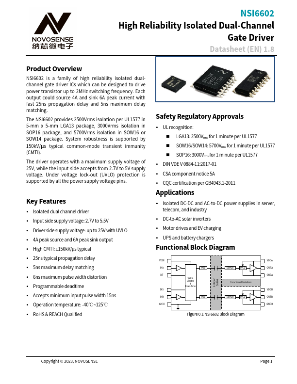
Datasheet4U Logo Datasheet4U.com

NSi6602 - High Reliability Isolated Dual-Channel Gate Driver

Datasheet Summary

Description

6.1.

INSULATION CHARACTERISTICS 16 6.2.

SAFETY-LIMITING VALUES 17 6.3.

Features

  • Isolated dual channel driver.
  • Input side supply voltage: 2.7V to 5.5V.
  • Driver side supply voltage: up to 25V with UVLO.
  • 4A peak source and 6A peak sink output.
  • High CMTI: ±150kV/μs typical.
  • 25ns typical propagation delay.
  • 5ns maximum delay matching.
  • 6ns maximum pulse width distortion.
  • Programmable deadtime.
  • Accepts minimum input pulse width 15ns.
  • Operation temperature: -40℃~125℃.
  • RoHS & REACH Qualified Safety Regulatory Approvals.

📥 Download Datasheet

Datasheet preview – NSi6602

Datasheet Details

Part number NSi6602
Manufacturer NOVOSENSE
File Size 2.62 MB
Description High Reliability Isolated Dual-Channel Gate Driver
Datasheet download datasheet NSi6602 Datasheet
Additional preview pages of the NSi6602 datasheet.
Other Datasheets by NOVOSENSE

Full PDF Text Transcription

Click to expand full text
NSI6602 High Reliability Isolated Dual-Channel Gate Driver Datasheet (EN) 1.8 Product Overview NSI6602 is a family of high reliability isolated dualchannel gate driver ICs which can be designed to drive power transistor up to 2MHz switching frequency. Each output could source 4A and sink 6A peak current with fast 25ns propagation delay and 5ns maximum delay matching. The NSI6602 provides 2500Vrms isolation per UL1577 in 5-mm x 5-mm LGA13 package, 3000Vrms isolation in SOP16 package, and 5700Vrms isolation in SOW16 or SOW14 package. System robustness is supported by 150kV/μs typical common-mode transient immunity (CMTI). The driver operates with a maximum supply voltage of 25V, while the input-side accepts from 2.7V to 5V supply voltage.
Published: |