- Part: C358C
- Description: UPC358
- Manufacturer: NEC
- Size: 74.77 KB
Key Features
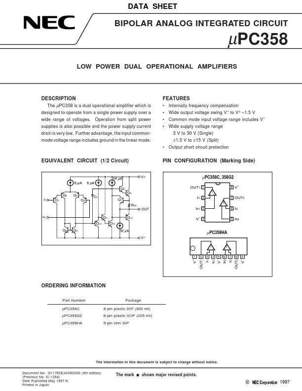
- Internally frequency compensation
- Wide output voltage swing V- to V+ -1.5 V
- Common mode input voltage range includes V-
- Wide supply voltage range 3 V to 30 V (Single) ±1.5 V to ±15 V (Split)
- Output short circuit protection
Datasheets by Manufacturer
- C3581 — Isahaya Electronics Corporation — 2SC3581
- C3514 — Inchange Semiconductor — Silicon NPN Power Transistor
- C3503 — SANYO — 2SC3503
- C3527 — Panasonic — 2SC3527
- C3502 — SANYO — 2SC3502
- C3563 — Inchange Semiconductor — 2SC3563
- C3507 — Panasonic — 2SC3507
- C3519 — Mospec Semiconductor — 2SC3519
- C3528 — SavantIC — 2SC3528
- C3505 — SavantIC — 2SC3505