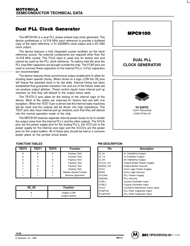
MPC9100 Overview
Key Specifications
Package: QFP
Operating Voltage: 3.3 V
Max Voltage (typical range): 3.6 V
Min Voltage (typical range): 3 V
Key Features
- a fully integrated crystal oscillator as the clock reference source
- No external components are required other than the 14.318 MHz crystal
- The TCLK input is used only for factory test and cannot be used as the PLL clock reference
- To reduce total die area the PLL loop filter capacitors are brought outside the chip
- The FCAP pins are used to connect these capacitors to the internal PLL’s
- 0.01µf capacitors are recommended
- The device features three synchronous output enable pins to allow for shutting down specific clocks
- When driven to a logic LOW the OE pins will freeze the selected clock in its low state
- Internal timing has been established that guarantee transition into and out of the freeze state will not produce output glitches
- These control inputs have internal pull up resistors so that they will default to the output active state