LX7169
® 3A Step-Down Converter
TM
PRODUCTION DATASHEET
DESCRIPTION
KEY FEATURES
LX7169 is a step-down PWM Switching Other features of the part are:
regulator IC with integrated high side P-
a) Cycle-by-cycle current limit
Channel and low side N-Channel followed by HICCUP mode which
MOSFETs. The IC operates using a reduces the overall power dissipation of
hysteretic control topology with a full load the internal MOSFETs
operating frequency of 3MHz. This
switching frequency allows for small output
filter components while maintaining
b) Thermal protection and internal
digital soft start.
excellent dynamic load response.
The LX7169 also provides a Power Good
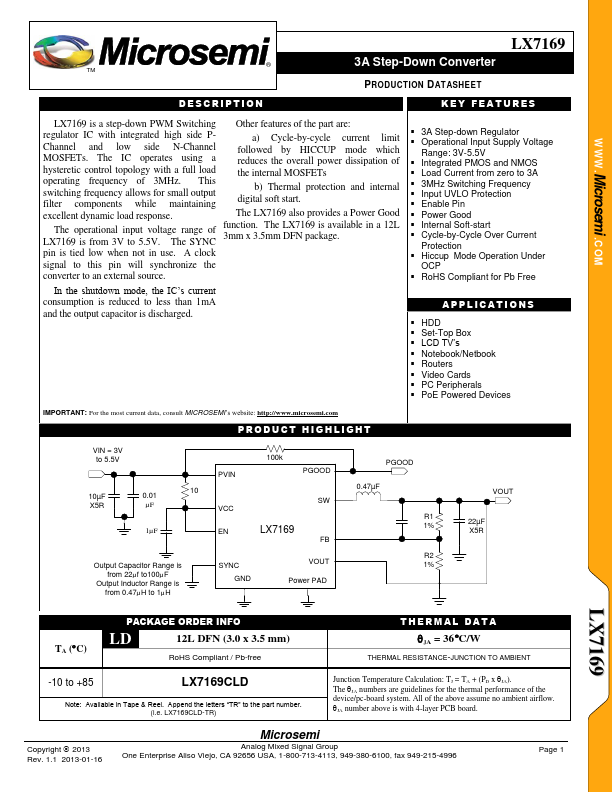
The operational input voltage range of
LX7169 is from 3V to 5.5V. The SYNC
function. The LX7169 is available in a 12L
3mm x 3.5mm DFN package.
pin is tied low when not in use. A clock
signal to this pin will synchronize the
converter to an external source.
In the shutdown mode, the IC’s current
consumption is reduced to less than 1mA
and the output capacitor is discharged.
3A Step-down Regulator
Operational Input Supply Voltage
Range: 3V-5.5V
Integrated PMOS and NMOS
Load Current from zero to 3A
3MHz Switching Frequency
Input UVLO Protection
Enable Pin
Power Good
Internal Soft-start
Cycle-by-Cycle Over Current
Protection
Hiccup Mode Operation Under
OCP
RoHS Compliant for Pb Free
APPLICATIONS
HDD
Set-Top Box
LCD TV’s
Notebook/Netbook
Routers
Video Cards
PC Peripherals
PoE Powered Devices
IMPORTANT: For the most current data, consult MICROSEMI’s website: http://www.microsemi.com
PRODUCT HIGHLIGHT
VIN = 3V
to 5.5V
10µF
X5R
0.01
µF
1µF
10
Output Capacitor Range is
from 22µf to100µF
Output Inductor Range is
from 0.47µH to 1µH
PVIN
100k
PGOOD
VCC
SW
EN LX7169
FB
SYNC
GND
VOUT
Power PAD
PGOOD
0.47µF
R1
1%
R2
1%
VOUT
22µF
X5R
TA (C)
PACKAGE ORDER INFO
LD 12L DFN (3.0 x 3.5 mm)
RoHS Compliant / Pb-free
THERMAL DATA
JA = 36C/W
THERMAL RESISTANCE-JUNCTION TO AMBIENT
-10 to +85
LX7169CLD
Note: Available in Tape & Reel. Append the letters “TR” to the part number.
(i.e. LX7169CLD-TR)
Junction Temperature Calculation: TJ = TA + (PD x JA).
The JA numbers are guidelines for the thermal performance of the
device/pc-board system. All of the above assume no ambient airflow.
JA number above is with 4-layer PCB board.
Copyright 2013
Rev. 1.1 2013-01-16
Microsemi
Analog Mixed Signal Group
One Enterprise Aliso Viejo, CA 92656 USA, 1-800-713-4113, 949-380-6100, fax 949-215-4996
Page 1