MT28F320A18
FEATURES
Low Voltage, Extended Temperature 0.15µm Process Technology
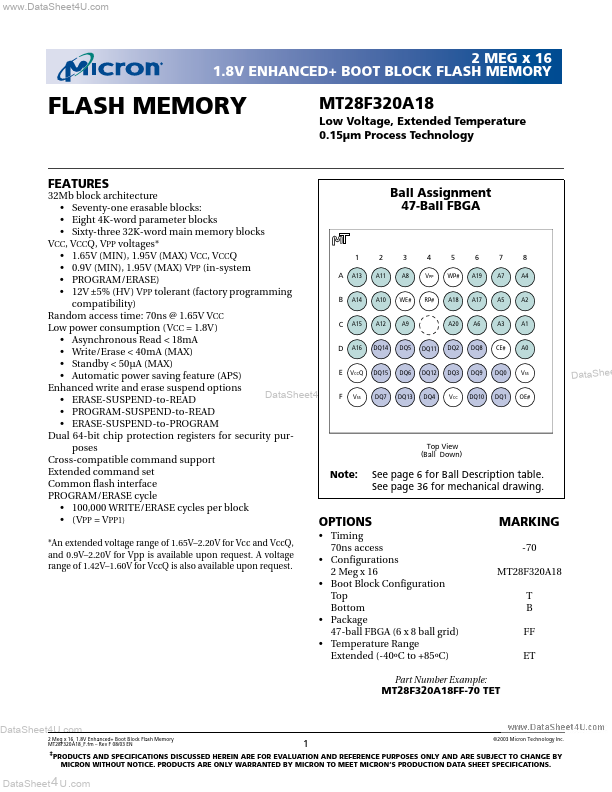
Ball Assignment 32Mb block architecture 47-Ball FBGA
- Seventy-one erasable blocks:
- Eight 4K-word parameter blocks
- Sixty-three 32K-word main memory blocks VCC, VCCQ, VPP voltages-
- 1.65V (MIN), 1.95V (MAX) VCC, VCCQ 1 2 3 4 5 6 7 8
- 0.9V (MIN), 1.95V (MAX) VPP (in-system WP# A4 VPP A8 A19 A11 A7 A A13
- PROGRAM/ERASE)
- 12V ±5% (HV) VPP tolerant (factory programming A18 A2 WE# A17 A10 RP# A5 B A14 patibility) Random access time: 70ns @ 1.65V VCC A20 A1 A9 A6 A12 A3 C A15 Low power consumption (VCC = 1.8V)
- Asynchronous Read < 18m A DQ2 A0 DQ5 DQ8 DQ14 CE# D A16 DQ11
- Write/Erase < 40m A (MAX)
- Standby < 50µA (MAX) DQ3 VSS DQ6 DQ9 DQ0 E VCCQ DQ15 DQ12
- Automatic power saving feature
(APS) Enhanced write and erase suspend options . VCC DQ13 DQ10 DQ7 DQ1 OE# F VSS DQ4
- ERASE-SUSPEND-to-READ
- PROGRAM-SUSPEND-to-READ
- ERASE-SUSPEND-to-PROGRAM Dual 64-bit chip protection registers for security pur...