Datasheet Details
| Part number | MT28F002B3 |
|---|---|
| Manufacturer | Micron Technology |
| File Size | 819.61 KB |
| Description | FLASH MEMORY |
| Datasheet |
 MT28F002B3 Datasheet MT28F002B3 Datasheet
|
|
|
Download the MT28F002B3 datasheet PDF. This datasheet also includes the MT28F200B3 variant, as both parts are published together in a single manufacturer document.
| Part number | MT28F002B3 |
|---|---|
| Manufacturer | Micron Technology |
| File Size | 819.61 KB |
| Description | FLASH MEMORY |
| Datasheet |
MT28F002B3 Datasheet
|
|
|
|
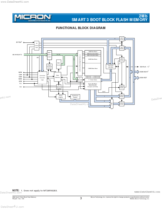
• Byte-wide READ and WRITE only The MT28F002B3 (x8) and MT28F200B3 (x16/x8) (MT28F002B3, 256K x 8) are nonvolatile, electrically block-erasable (flash), pro• TSOP and SOP packaging options grammable, read-only memories containing 2,097,152 bits organized as 131,072 words (16 bits) or 262,144 OPTIONS MARKING bytes (8 bits).
Writing or erasing the device is done with • Timing either a 3.3V or 5V VPP voltage, while all operations are 90ns access -9 performed with a 3.3V VCC.
Due to process technology 100ns access -10 ET advances, 5V VPP is optimal for application and produc• Configurations tion programming.
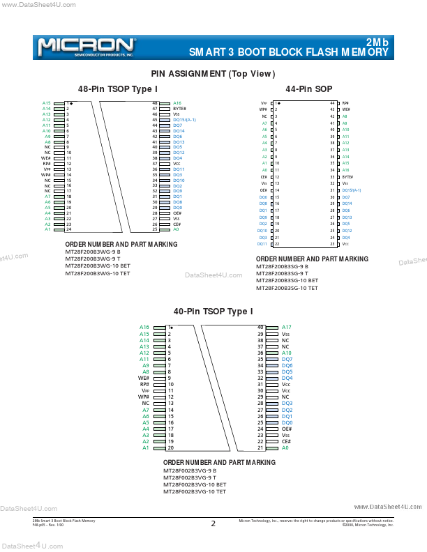
www.DataSheet4U.com 2Mb SMART 3 BOOT BLOCK FLASH MEMORY FLASH MEMORY MT28F002B3 MT28F200B3 3V Only, Dual Supply (Smart 3) 40-Pin TSOP Type I 48-Pin TSOP Type I • Five erase blocks: 16KB/8K-word boot block (protected) Two 8KB/4K-word parameter blocks Two main memory blocks • Smart 3 technology (B3): 3.3V ± 0.3V VCC 3.3V ± 0.3V VPP application programming 5V ±10% VPP application/production programming 44-Pin SOP 12V ± 5% VPP compatibility production programming • Address access times: 90ns, 100ns • 100,000 ERASE cycles • Industry-standard pinouts • Inputs and outputs are fully TTL-compatible ee DataSh • Automated write and erase algorithm • Two-cycle WRITE/ERASE sequence DataSheet4U.
| Part Number | Description |
|---|---|
| MT28F002B5 | FLASH MEMORY |
| MT28F004B3 | FLASH MEMORY |
| MT28F004B5 | SMART 5 BOOT BLOCK FLASH MEMORY |
| MT28F008B3 | FLASH MEMORY |
| MT28F008B5 | (MT28F008B5 / MT28F800B5) FLASH MEMORY |
| MT28F016S5 | 2 MEG x 8 SMART 5 EVEN-SECTORED FLASH MEMORY |
| MT28F1284W18 | 1.8V Low Voltage Extended Temperature |
| MT28F128J3 | Q-FLASH MEMORY |
| MT28F160A3 | FLASH MEMORY |
| MT28F160C3 | FLASH MEMORY |