LTC6754 Datasheet Text
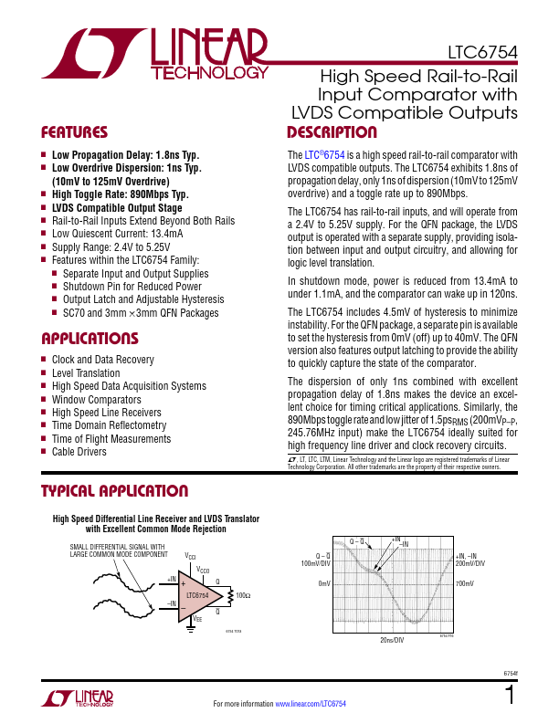
Features nn Low Propagation Delay: 1.8ns Typ. nn Low Overdrive Dispersion: 1ns Typ.
(10mV to 125mV Overdrive) nn High Toggle Rate: 890Mbps Typ. nn LVDS patible Output Stage nn Rail-to-Rail Inputs Extend Beyond Both Rails nn Low Quiescent Current: 13.4mA nn Supply Range: 2.4V to 5.25V nn Features within the LTC6754 Family: nn Separate Input and Output Supplies nn Shutdown Pin for Reduced Power nn Output Latch and Adjustable Hysteresis nn SC70 and 3mm × 3mm QFN Packages
Applications nn Clock and Data Recovery nn Level Translation nn High Speed Data Acquisition Systems nn Window parators nn High Speed Line Receivers nn Time Domain Reflectometry nn Time of Flight Measurements nn Cable Drivers
Typical Application
High Speed Differential Line Receiver and LVDS Translator with Excellent mon Mode Rejection
SMALL DIFFERENTIAL SIGNAL WITH LARGE MON MODE PONENT
VCCI
+IN +
VCCO Q
LTC6754
- IN
- VEE
Q
100Ω
6754 T01a
LTC6754 High Speed Rail-to-Rail Input parator with LVDS patible Outputs Description
The LTC®6754 is a high speed rail-to-rail parator with LVDS patible outputs. The LTC6754 exhibits 1.8ns of propagation delay, only 1ns of dispersion (10mV to 125mV overdrive) and a toggle rate up to 890Mbps. The LTC6754 has rail-to-rail inputs, and will operate from a 2.4V to 5.25V supply. For the QFN package, the LVDS output is operated with a separate supply, providing isolation between input and output circuitry, and allowing for logic level translation. In shutdown mode, power is reduced from 13.4mA to under 1.1mA, and the parator can wake up in 120ns. The LTC6754 includes 4.5mV of hysteresis to minimize instability. For the QFN package, a separate pin is available to set the hysteresis from 0mV (off) up to 40mV. The QFN version also Features...