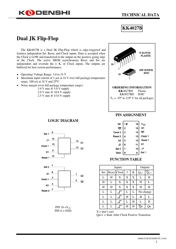
• Part: KK4027B
  • Description: Dual JK Flip-Flop
  • Manufacturer: Kodenshi AUK Group
  • Size: 433.24 KB
Download KK4027B Datasheet PDF
Kodenshi AUK Group
KK4027B
features independent Set, Reset, and Clock inputs. Data is accepted when the Clock is LOW and transferred to the output on the positive-going edge of the Clock. The active HIGH asynchronous Reset and Set are independent and override the J, K, or Clock inputs. The outputs are buffered for best system performance. - Operating Voltage Range: 3.0 to 18 V - Maximum input current of 1 µA at 18 V over full package-temperature range; 100 n A at 18 V and 25°C - Noise margin (over full package temperature range): 1.0 V min @ 5.0 V supply 2.0 V min @ 10.0 V supply 2.5 V min @ 15.0 V supply ORDERING INFORMATION KK4027BN Plastic KK4027BD SOIC TA = -55° to 125° C for all packages PIN ASSIGNMENT LOGIC DIAGRAM FUNCTION TABLE Inputs Set Reset Clock L H H L L L PIN 16 =VCC PIN 8 = GND L H L H L L L L X X X J X X X L H L H K X X X L L H H Outputs Qn+1 L H H H L Qn Qn+1 H L H L H Qn No change X = don’t care Qn+1 = State After Clock Positive Transition .. MAXIMUM RATINGS- Symbol VCC VIN...