Datasheet Details
| Part number | EL2033 |
|---|---|
| Manufacturer | Intersil (now Renesas) |
| File Size | 365.50 KB |
| Description | 100MHz Video Line Driver |
| Download | EL2033 Download (PDF) |
|
|
Download the EL2033 datasheet PDF. This datasheet also includes the EL2003 variant, as both parts are published together in a single manufacturer document.
| Part number | EL2033 |
|---|---|
| Manufacturer | Intersil (now Renesas) |
| File Size | 365.50 KB |
| Description | 100MHz Video Line Driver |
| Download | EL2033 Download (PDF) |
|
|
|
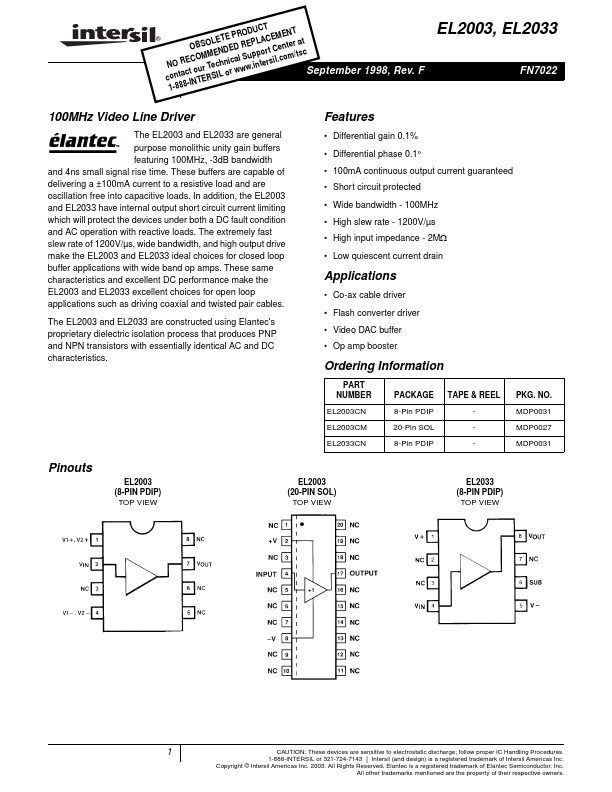
® cN1oO-n8t8Ra8cE-tIOCDNoBOTuaSMErtORTMaLeSEcEISNLhTDnhEoiErcePDaweRlwROtSwEuD.PpUinLpCtAoeTrCrtsECilM.ecEnotNmeTr/tastcSeptember 1998, Rev.
F EL2003, EL2033 FN7022 100MHz Video Line Driver The EL2003 and EL2033 are general purpose monolithic unity gain buffers featuring 100MHz, -3dB bandwidth and 4ns small signal rise time.
These buffers are capable of delivering a ±100mA current to a resistive load and are oscillation free into capacitive loads.
| Brand Logo | Part Number | Description | Manufacturer |
|---|---|---|---|
| EL2033C | 100MHz Video Line Driver | Elantec |
| Part Number | Description |
|---|---|
| EL2001 | 70MHz Buffer Amplifier |
| EL2002 | 180MHz Buffer Amplifier |
| EL2003 | 100MHz Video Line Driver |
| EL2019 | High Voltage Comparator |
| EL2044 | Low Power/Low Voltage 120MHz Unity-Gain Stable Operational Amplifier |
| EL2045 | Operational Amplifier |
| EL2072 | 730MHz Closed Loop Buffer |
| EL2073 | 200MHz Unity-Gain Stable Operational Amplifier |
| EL2074 | 400MHz GBWP Gain-of-2 Stable Operational Amplifier |
| EL2082 | Current-Mode Multiplier |