Datasheet4U Logo Datasheet4U.com

IS43R32160E - 512Mb DDR SDRAM

Download the IS43R32160E datasheet PDF. This datasheet also covers the IS43R86400E variant, as both devices belong to the same 512mb ddr sdram family and are provided as variant models within a single manufacturer datasheet.

Description

x8 A0-A12 Row Address Input A0-A9, A11 Column Address Input BA0, BA1 Bank Select Address DQ0 DQ7 Data I/O CK, CK System Clock Input CKE Clock Enable CS Chip Select CAS Column Address Strobe Command RAS Row Address Strobe Command WE Write Enable 4 66 VSS 65 DQ7 64 VSSQ

Features

  • VDD and VDDQ: 2.5V ± 0.2V (-5, -6).
  • VDD and VDDQ: 2.5V ± 0.1V (-4).
  • SSTL_2 compatible I/O.
  • Double-data rate architecture; two data transfers per clock cycle.
  • Bidirectional, data strobe (DQS) is transmitted/ received with data, to be used in capturing data at the receiver.
  • DQS is edge-aligned with data for READs and centre-aligned with data for WRITEs.
  • Differential clock inputs (CK and CK).
  • DLL aligns DQ and DQS tran.

📥 Download Datasheet

Note: The manufacturer provides a single datasheet file (IS43R86400E-IntegratedSiliconSolution.pdf) that lists specifications for multiple related part numbers.

Full PDF Text Transcription (Reference)

The following content is an automatically extracted verbatim text from the original manufacturer datasheet and is provided for reference purposes only.

View original datasheet text
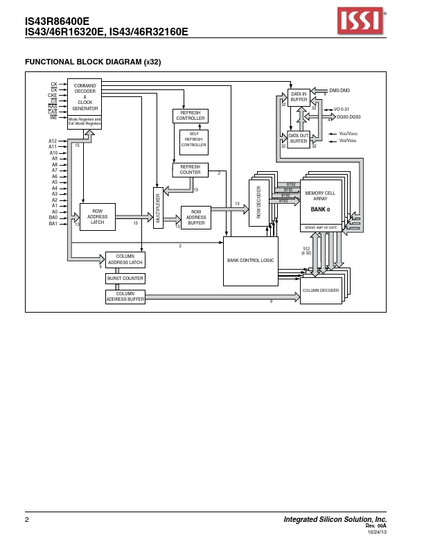
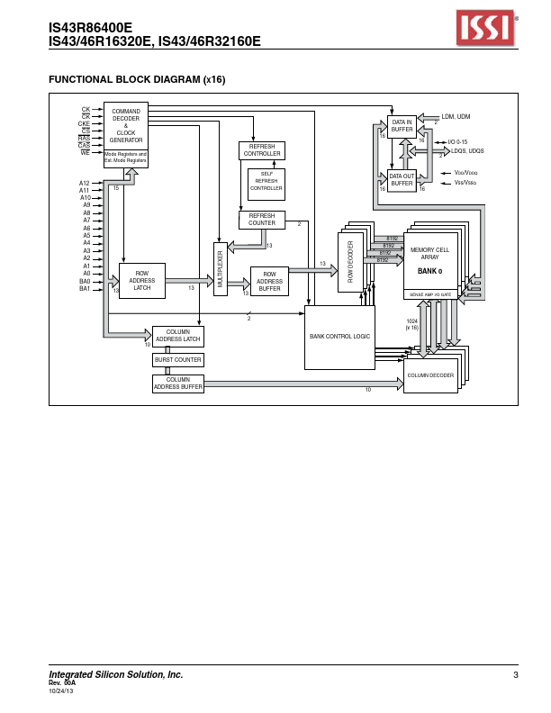
IS43R86400E IS43/46R16320E, IS43/46R32160E 16Mx32, 32Mx16, 64Mx8 ADVANCED INFORMATION 512Mb DDR SDRAM NOVEMBER 2013 FEATURES • VDD and VDDQ: 2.5V ± 0.2V (-5, -6) • VDD and VDDQ: 2.5V ± 0.1V (-4) • SSTL_2 compatible I/O • Double-data rate architecture; two data transfers per clock cycle • Bidirectional, data strobe (DQS) is transmitted/ received with data, to be used in capturing data at the receiver • DQS is edge-aligned with data for READs and centre-aligned with data for WRITEs • Differential clock inputs (CK and CK) • DLL aligns DQ and DQS transitions with CK transitions • Commands entered on each positive CK edge; data and data mask referenced to both edges of DQS • Four internal banks for concurrent operation • Data Mask for write data.
Published: |