Datasheet Details
| Part number | QS532807 |
|---|---|
| Manufacturer | Integrated Device Technology |
| File Size | 95.04 KB |
| Description | GUARANTEED LOW SKEW CMOS CLOCK DRIVER/BUFFER |
| Datasheet |
 QS532807 Datasheet QS532807 Datasheet
|
|
|
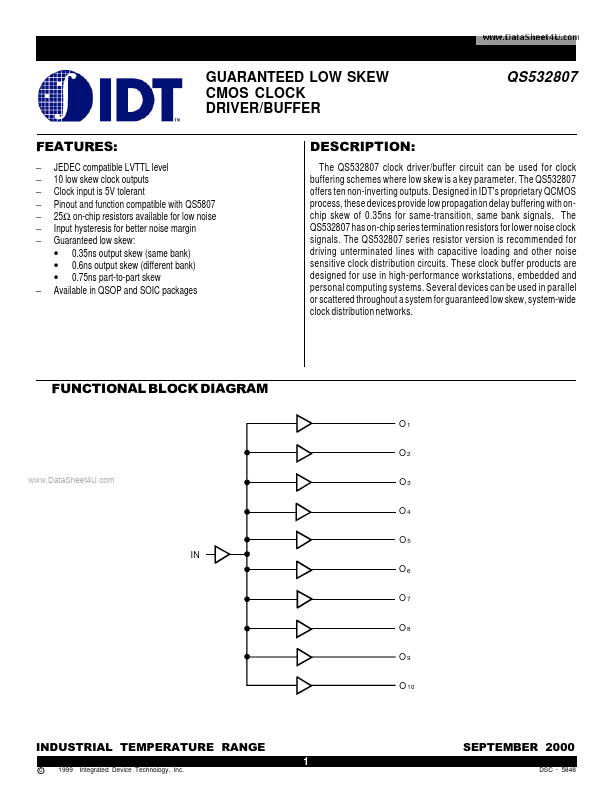
The QS532807 clock driver/buffer circuit can be used for clock buffering schemes where low skew is a key parameter.
The QS532807 offers ten non-inverting outputs.
| Part number | QS532807 |
|---|---|
| Manufacturer | Integrated Device Technology |
| File Size | 95.04 KB |
| Description | GUARANTEED LOW SKEW CMOS CLOCK DRIVER/BUFFER |
| Datasheet |
QS532807 Datasheet
|
|
|
|