Datasheet4U Logo Datasheet4U.com

IDT5T9306 - 2.5V LVDS 1:6 CLOCK BUFFER TERABUFFER II

Description

The IDT5T9306 2.5V differential clock buffer is a user-selectable differential input to six LVDS outputs.

The fanout from a differential input to six LVDS outputs reduces loading on the preceding driver and provides an efficient clock distribution network.

Features

  • Guaranteed Low Skew < 25ps (max) Very low duty cycle distortion < 125ps (max) High speed propagation delay < 1.75ns (max) Additive phase jitter, RMS 0.159ps (typical) @ 125MHz Up to 1GHz operation Selectable inputs Hot insertable and over-voltage tolerant inputs 3.3V / 2.5V LVTTL, HSTL, eHSTL,.

📥 Download Datasheet

Datasheet Details

Part number IDT5T9306
Manufacturer Integrated Device Technology
File Size 244.95 KB
Description 2.5V LVDS 1:6 CLOCK BUFFER TERABUFFER II
Datasheet download datasheet IDT5T9306 Datasheet

Full PDF Text Transcription (Reference)

The following content is an automatically extracted verbatim text from the original manufacturer datasheet and is provided for reference purposes only.

View original datasheet text
www.DataSheet4U.com 2.5V LVDS 1:6 CLOCK BUFFER TERABUFFER™ II FEATURES: • • • • • • • • • • • • Guaranteed Low Skew < 25ps (max) Very low duty cycle distortion < 125ps (max) High speed propagation delay < 1.75ns (max) Additive phase jitter, RMS 0.159ps (typical) @ 125MHz Up to 1GHz operation Selectable inputs Hot insertable and over-voltage tolerant inputs 3.3V / 2.5V LVTTL, HSTL, eHSTL, LVEPECL (2.5V), LVPECL (3.3V), CML, or LVDS input interface Selectable differential inputs to six LVDS outputs Power-down mode 2.5V VDD Available in VFQFPN package
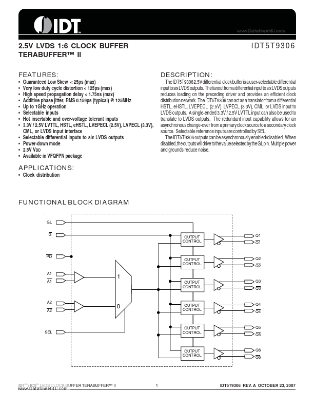
 IDT5T9306 DESCRIPTION: The IDT5T9306 2.5V differential clock buffer is a user-selectable differential input to six LVDS outputs.
Published: |