Datasheet Details
| Part number | ICS650-40 |
|---|---|
| Manufacturer | Integrated Circuit Systems |
| File Size | 147.59 KB |
| Description | ETHERNET SWITCH CLOCK SOURCE |
| Datasheet |
 ICS650-40 Datasheet ICS650-40 Datasheet
|
|
|
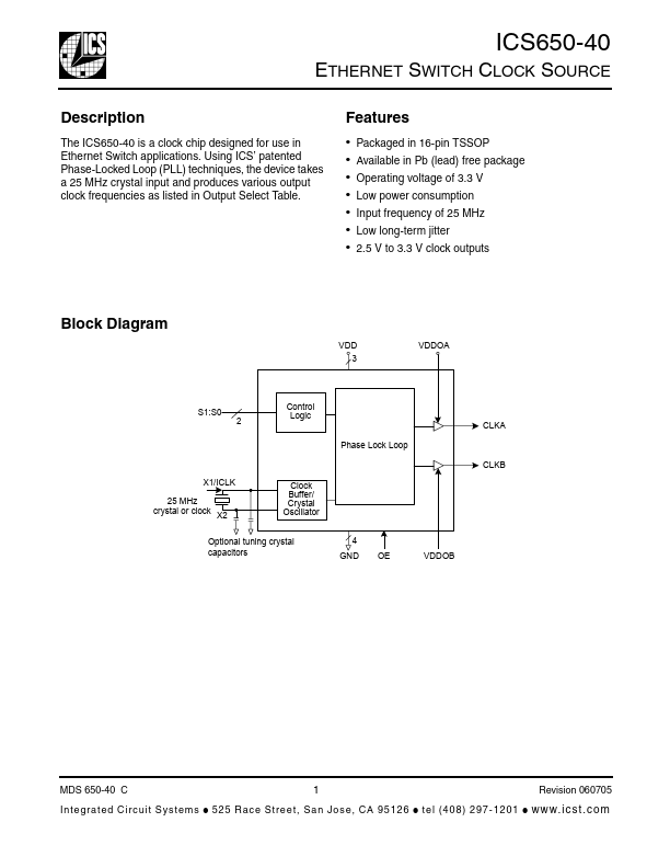
The ICS650-40 is a clock chip designed for use in Ethernet Switch applications.
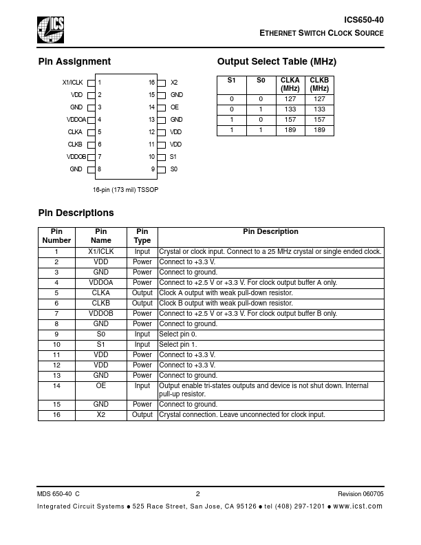
Using ICS’ patented Phase-Locked Loop (PLL) techniques, the device takes a 25 MHz crystal input and produces various output clock frequencies as listed in Output Select Table.
| Part number | ICS650-40 |
|---|---|
| Manufacturer | Integrated Circuit Systems |
| File Size | 147.59 KB |
| Description | ETHERNET SWITCH CLOCK SOURCE |
| Datasheet |
ICS650-40 Datasheet
|
|
|
|
| Part Number | Description | Manufacturer |
|---|---|---|
| ICS650-40A | ETHERNET SWITCH CLOCK SOURCE | Renesas |
| ICS650-41 | SPREAD SPECTRUM CLOCK SYNTHESIZER | IDT |
| ICS650-44 | SPREAD SPECTRUM CLOCK SYNTHESIZER | Renesas |
| ICS650-44 | SPREAD SPECTRUM CLOCK SYNTHESIZER | IDT |
| ICS650-01 | SYSTEM PERIPHERAL CLOCK SOURCE | Renesas |
| Part Number | Description |
|---|---|
| ICS650-47 | Spread Spectrum Clock Synthesizer |
| ICS650-01B | System Peripheral Clock Source |
| ICS650-05 | HDTV Clock Synthesizer |
| ICS650-07B | Broadcom Clock Source |
| ICS650-07C | Networking Clock Source |
The following content is an automatically extracted verbatim text from the original manufacturer datasheet and is provided for reference purposes only.