Datasheet Details
| Part number | IS61LF51218 |
|---|---|
| Manufacturer | ISSI (now Infineon) |
| File Size | 220.51 KB |
| Description | (IS61LF25632 / IS61LF25636 / IS61LF51218) 256Kx32 Synchronous Flow-through Static RAM |
| Datasheet |
 IS61LF51218 Datasheet IS61LF51218 Datasheet
|
|
|
Download the IS61LF51218 datasheet PDF. This datasheet also covers the IS61LF25632 variant, as both devices belong to the same (is61lf25632 / is61lf25636 / is61lf51218) 256kx32 synchronous flow-through static ram family and are provided as variant models within a single manufacturer datasheet.
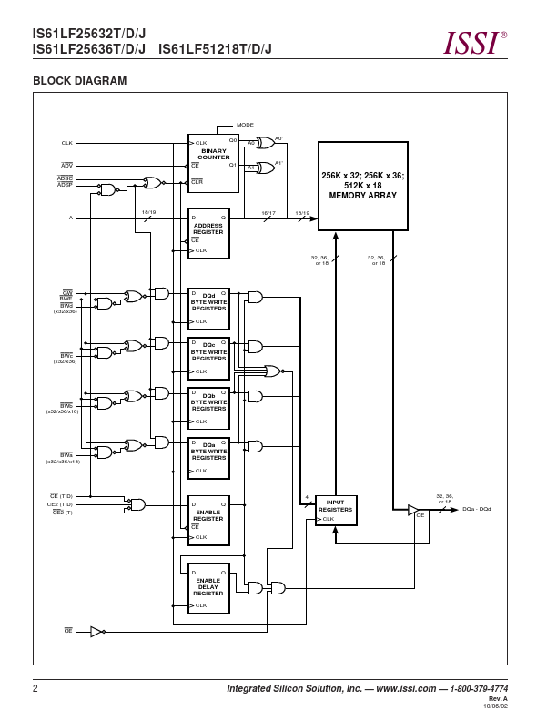
The ISSI IS61LF25632, IS61LF25636, and IS61LF51218 are high-speed, low-power synchronous static RAMs designed to provide a burstable, high-performance and memories for commucation and networking applications.
| Part number | IS61LF51218 |
|---|---|
| Manufacturer | ISSI (now Infineon) |
| File Size | 220.51 KB |
| Description | (IS61LF25632 / IS61LF25636 / IS61LF51218) 256Kx32 Synchronous Flow-through Static RAM |
| Datasheet |
IS61LF51218 Datasheet
|
|
|
|
| Part Number | Description | Manufacturer |
|---|---|---|
| IS61LF51218A | 256K x 36-512K x 18 9Mb SYNCHRONOUS FLOW-THROUGH STATIC RAM | Integrated Silicon Solution |
| IS61LF25636A | 256K x 36-512K x 18 9Mb SYNCHRONOUS FLOW-THROUGH STATIC RAM | Integrated Silicon Solution |
| IS61LF6432A | SYNCHRONOUS FLOW-THROUGH STATIC RAM | Integrated Silicon Solution |
| IS61LF6436A | SYNCHRONOUS FLOW-THROUGH STATIC RAM | Integrated Silicon Solution |
| IS61LP6432A | 64K x 32 or 64K x 36 SYNCHRONOUS PIPELINED STATIC RAM | Integrated Silicon Solution |
| Part Number | Description |
|---|---|
| IS61LF51236A | (IS61xFxxxxxA) Synchronous Flow-through Static RAM |
| IS61LF102418A | (IS61xFxxxxxA) Synchronous Flow-through Static RAM |
| IS61LF12832A | (IS6xxFxxxxxA) Synchronous Flow-through Static RAM |
| IS61LF12832EC | SYNCHRONOUS FLOW-THROUGH SRAM |
| IS61LF12836A | (IS6xxFxxxxxA) Synchronous Flow-through Static RAM |
The following content is an automatically extracted verbatim text from the original manufacturer datasheet and is provided for reference purposes only.