Datasheet Details
| Part number | IS45RM32160E |
|---|---|
| Manufacturer | ISSI (now Infineon) |
| File Size | 592.91 KB |
| Description | 4M x 32Bits x 4Banks Mobile Synchronous DRAM |
| Datasheet |
 IS45RM32160E Datasheet IS45RM32160E Datasheet
|
|
|
Download the IS45RM32160E datasheet PDF. This datasheet also covers the IS42SM32160E variant, as both devices belong to the same 4m x 32bits x 4banks mobile synchronous dram family and are provided as variant models within a single manufacturer datasheet.
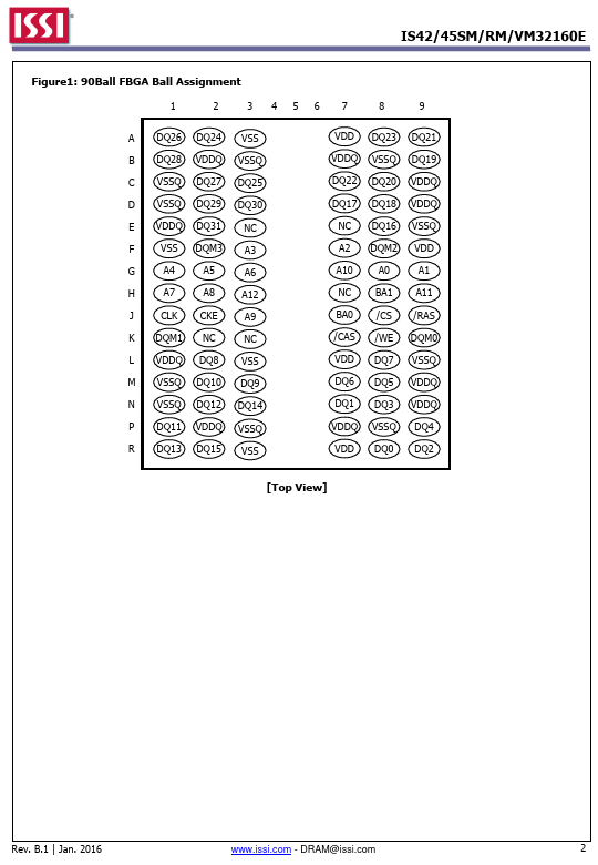
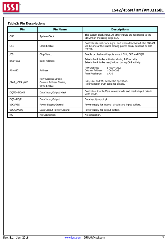
These IS42/45SM/RM/VM32160E are mobile 536,870,912 bits CMOS Synchronous DRAM organized as 4 banks of 4,194,304 words x 32 bits.
These products are offering fully synchronous operation and are referenced to a positive edge of the clock.
| Part number | IS45RM32160E |
|---|---|
| Manufacturer | ISSI (now Infineon) |
| File Size | 592.91 KB |
| Description | 4M x 32Bits x 4Banks Mobile Synchronous DRAM |
| Datasheet |
IS45RM32160E Datasheet
|
|
|
|
| Part Number | Description | Manufacturer |
|---|---|---|
| IS450 | OPIC LIGHT DETECTOR WITH BULLT-IN SIGNAL PROCESSING CIRCULT FOR LIGHT MODULATION SYSTEM | Sharp Electrionic Components |
| IS455 | Linear Output Type OPIC Light Detector | Sharp Electrionic Components |
| IS456 | High Speed Response Type OPIC Light Detector | Sharp Electrionic Components |
| IS457 | High Speed Response Type OPIC Light Detector | Sharp Electrionic Components |
| IS45LV44002B | DYNAMIC RAM | Integrated Silicon Solution |
| Part Number | Description |
|---|---|
| IS45RM32100D | 512K x 32Bits x 2Banks Low Power Synchronous DRAM |
| IS45RM32200M | 512K x 32Bits x 4Banks Mobile Synchronous DRAM |
| IS45RM32400G | 1M x 32Bits x 4Banks Mobile Synchronous DRAM |
| IS45RM32400H | 1M x 32Bits x 4Banks Mobile Synchronous DRAM |
| IS45RM32800E | 2M x 32Bits x 4Banks Mobile Synchronous DRAM |
The following content is an automatically extracted verbatim text from the original manufacturer datasheet and is provided for reference purposes only.