Datasheet Details
| Part number | IDT71V25761S |
|---|---|
| Manufacturer | IDT |
| File Size | 261.85 KB |
| Description | 128K x 36 3.3V Synchronous SRAMs |
| Datasheet |
 IDT71V25761S Datasheet IDT71V25761S Datasheet
|
|
|
Download the IDT71V25761S datasheet PDF. This datasheet also covers the IDT71V25761YS variant, as both devices belong to the same 128k x 36 3.3v synchronous srams family and are provided as variant models within a single manufacturer datasheet.
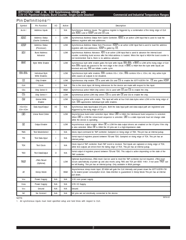
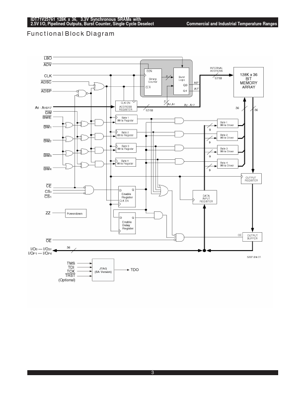
The IDT71V25761 are high-speed SRAMs organized as 128K x 36.
The IDT71V25761 SRAMs contain write, data, address and control registers.
| Part number | IDT71V25761S |
|---|---|
| Manufacturer | IDT |
| File Size | 261.85 KB |
| Description | 128K x 36 3.3V Synchronous SRAMs |
| Datasheet |
IDT71V25761S Datasheet
|
|
|
|
| Part Number | Description | Manufacturer |
|---|---|---|
| IDT71V2576S | 128K X 36/ 256K X 18 3.3V Synchronous SRAMs 2.5V I/O/ Pipelined Outputs/ Burst Counter/ Single Cycle Deselect | Integrated Device Technology |
| IDT71V2576SA | 128K X 36/ 256K X 18 3.3V Synchronous SRAMs 2.5V I/O/ Pipelined Outputs/ Burst Counter/ Single Cycle Deselect | Integrated Device Technology |
| IDT71V2578S | 128K X 36/ 256K X 18 3.3V Synchronous SRAMs 2.5V I/O/ Pipelined Outputs/ Burst Counter/ Single Cycle Deselect | Integrated Device Technology |
| IDT71V2578SA | 128K X 36/ 256K X 18 3.3V Synchronous SRAMs 2.5V I/O/ Pipelined Outputs/ Burst Counter/ Single Cycle Deselect | Integrated Device Technology |
| IDT71V2546SA | 128K x 36/ 256K x 18 3.3V Synchronous ZBT SRAMs 2.5V I/O/ Burst Counter Pipelined Outputs | Integrated Device Technology |
| Part Number | Description |
|---|---|
| IDT71V25761 | (IDT71V25761 / IDT71V25781) Synchronous SRAMs |
| IDT71V25761YS | 128K x 36 3.3V Synchronous SRAMs |
| IDT71V2577 | (IDT71V2577 / IDT71V2579) Synchronous SRAMs |
| IDT71V2577S | (IDT71V2577S / IDT71V25779) Synchronous SRAMs |
| IDT71V2577SA | (IDT71V2577S / IDT71V25779) Synchronous SRAMs |
The following content is an automatically extracted verbatim text from the original manufacturer datasheet and is provided for reference purposes only.