Datasheet4U Logo Datasheet4U.com

K2115 - 2SK2115

Download the K2115 datasheet PDF. This datasheet also covers the K2114 variant, as both devices belong to the same 2sk2115 family and are provided as variant models within a single manufacturer datasheet.
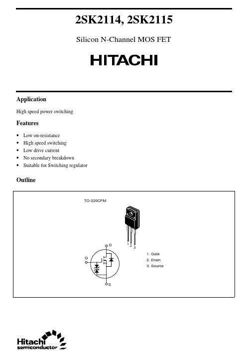
Features

  • Low on-resistance.
  • High speed switching.
  • Low drive current.
  • No secondary breakdown.
  • Suitable for Switching regulator Outline TO-220CFM D 12 3 1. Gate G 2. Drain 3. Source S 2SK2114, 2SK2115 Absolute Maximum Ratings (Ta = 25°C) Item Drain to source voltage 2SK2114 2SK2115 Gate to source voltage Drain current Drain peak current Body to drain diode reverse drain current Channel dissipation Channel temperature Storage temperature Notes 1. P.

📥 Download Datasheet

Note: The manufacturer provides a single datasheet file (K2114-HitachiSemiconductor.pdf) that lists specifications for multiple related part numbers.

Full PDF Text Transcription (Reference)

The following content is an automatically extracted verbatim text from the original manufacturer datasheet and is provided for reference purposes only.

View original datasheet text
2SK2114, 2SK2115 Silicon N-Channel MOS FET Application High speed power switching Features • Low on-resistance • High speed switching • Low drive current • No secondary breakdown • Suitable for Switching regulator Outline TO-220CFM D 12 3 1. Gate G 2. Drain 3. Source S 2SK2114, 2SK2115 Absolute Maximum Ratings (Ta = 25°C) Item Drain to source voltage 2SK2114 2SK2115 Gate to source voltage Drain current Drain peak current Body to drain diode reverse drain current Channel dissipation Channel temperature Storage temperature Notes 1. PW ≤ 10 µs, duty cycle ≤ 1 % 2.
Published: |