Description
The HD74ALVC16834 is an 18-bit universal bus driver designed for 2.3 V to 3.6 V VCC operation.
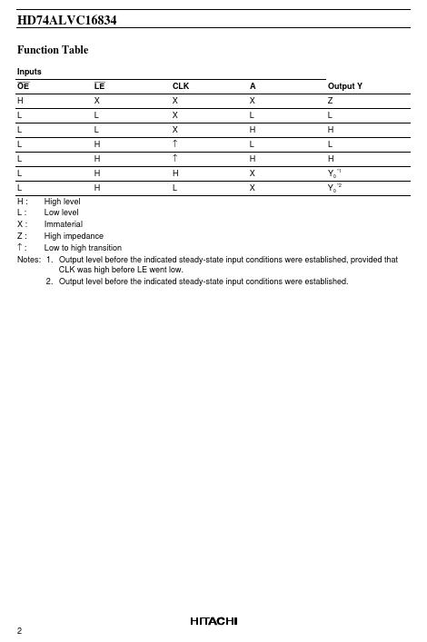
Data flow from A to Y is controlled by output enable (OE).
The device operates in the transparent mode when the latch enable ( LE) input is low.
Features
- Meets “PC SDRAM registered DIMM design support document, Rev. 1.2”.
- Typical VOL ground bounce < 0.8 V (@VCC = 3.3 V, Ta = 25°C).
- Typical VOH undershoot > 2.0 V (@VCC = 3.3 V, Ta = 25°C).
- High output current ±24 mA (@V CC = 3.0 V)
HD74ALVC16834
Function Table
Inputs OE H L L L L L L H: L: X: Z: ↑: Notes: LE X L L H H H H CLK X X X ↑ ↑ H L A X L H L H X X Output Y Z L H L H Y0.
- 1 Y0.
- 2
High level Low level Immaterial High impedance Low to high transit.
 HD74ALVC16834 Datasheet