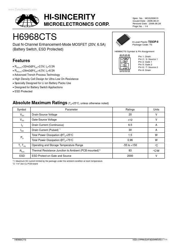
H6968CTS
Features
- RDS(on)<32mΩ@VGS=2.5V, ID=5.5A
- RDS(on)<24mΩ@VGS=4.5V, ID=6.5A
- Advanced Trench Process Technology
- High Density Cell Design for Ultra Low On-Resistance
- Specially Designed for Li ion Battery Packs Use
- Designed for Battery Switch Appliactions
- ESD Protected
Q2 Q1
Absolute Maximum Ratings (T =25 C, unless otherwise noted) o A
Symbol VDS VGS ID IDM PD Tj, Tstg RθJA ESD Drain-Source Voltage Gate-Source Voltage Drain Current (Continuous) Drain Current (Pulsed)
- 1
Parameter
Ratings 20 ±12 6.5 30
Units V V A A W W °C °C/W V
Total Power Dissipation @TA=25 C Total Power Dissipation @TA=75o C Operating and Storage Temperature Range Thermal Resistance Junction to Ambient (PCB mounted) ESD Protect on Gate and Source
- 2 o
1.5 0.96 -55 to +150 83 2000
- 1: Maximum DC current limited by the package under the ambient condition at room temperature.
- 2: 1-in2 2oz Cu PCB board
HSMC Product Specification
..
HI-SINCERITY
MICROELECTRONICS CORP.
Electrical...