HWL26NPB
Features
- Plastic Packaged Ga As Power FET
- Suitable for mercial Wireless
Applications
- High Efficiency
- 3V to 6V Operation
Description
The HWL26NPB is a medium Power Ga As FET using surface mount type plastic package for various L-Band applications. It is suitable for various 900 MHz, 1900 MHz cellular/wireless applications.
L-Band Ga As Power FET
Autumn 2002 V1
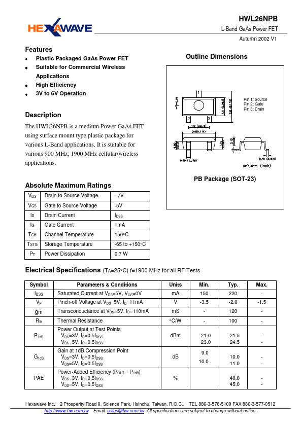
Outline Dimensions
1 23
Pin 1: Source Pin 2: Gate Pin 3: Drain
Absolute Maximum Ratings
VDS Drain to Source Voltage
+7V
VGS Gate to Source Voltage
-5V
ID Drain Current IG Gate Current
IDSS 1m A
TCH Channel Temperature
150°C
TSTG Storage Temperature
-65 to +150°C
PT Power Dissipation
0.7 W
PB Package (SOT-23)
Electrical Specifications (TA=25°C) f=1900 MHz for all RF Tests
Symbol IDSS VP gm
Rth
P1d B
G1d B
Parameters & Conditions
Saturated Current at VDS=5V, VGS=0V
Pinch-off Voltage at VDS=5V, ID=11m A
Transconductance at VDS=5V, ID=110m A
Thermal Resistance
Power Output at Test Points VDS=3V,...