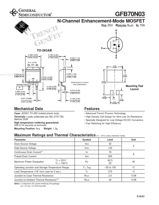
High Density Cell Design for Ultra Low On-Resistance.
Specially Designed for Low Voltage DC/DC Converters.
Fast Switching for High Efficiency
Maximum Ratings and Thermal Characteristics (T
Parameter Drain-Source Voltage Gate-Source Voltage Continuous Drain Current(1) Pulsed Drain Current Maximum Power Dissipation TC = 25°C TC = 100°C Symbol VDS VGS ID IDM PD TJ, Tstg TL RθJC
(2)
C
= 25°C unless otherwise noted)
Limit 30.
Other Datasheets by General Semiconductor (now Vishay)
Part Number
Description
Full PDF Text Transcription (Reference)
The following content is an automatically extracted verbatim text
from the original manufacturer datasheet and is provided for reference purposes only.
View original datasheet text
GFB70N03
N-Channel Enhancement-Mode MOSFET
H C N T E TRE NF E G
TO-263AB
0.380 (9.65) 0.420 (10.67) 0.21 (5.33) Min.
D
VDS 30V RDS(ON) 8mΩ ID 70A
D
®
G
0.160 (4.06) 0.190 (4.83)
0.045 (1.14) 0.055 (1.40)
S
0.42 (10.66)
0.320 (8.13) www.DataSheet4U.com 0.360 (9.14)
G PIN D S
0.575 (14.60) 0.625 (15.88)
0.055 (1.39) 0.066 (1.68)
Dimensions in inches and (millimeters)
0.63 (17.02)
0.33 (8.38)
Seating Plate
-T0.096 (2.43) 0.102 (2.59) 0.027 (0.686) 0.037 (0.940)
0.120 (3.05) 0.155 (3.94)
0.014 (0.35) 0.020 (0.51) 0.100 (2.54) 0.130 (3.30)
0.08 (2.032) 0.24 (6.096) 0.12 (3.
 70N03 Datasheet