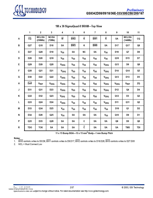
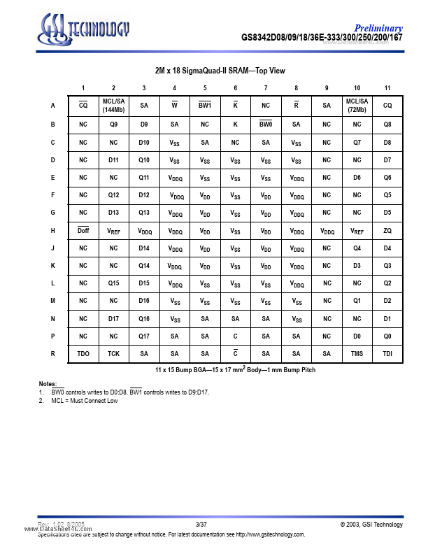
Table Symbol
SA NC R W BW0
BW3 NW0
NW1 K K C C TMS TDI TCK TDO VREF ZQ Qn Dn Doff CQ CQ VDD VDDQ VSS Note: NC = Not Connected to die or any other pin
Description
Synchronous Address Inputs No Connect Synchronous Read Synchronous Write Synchronous Byte Writes Nybble Write Control Pin
Full PDF Text Transcription for GS8342D08E-333 (Reference)
Note: Below is a high-fidelity text extraction (approx. 800 characters) for
GS8342D08E-333. For precise diagrams, and layout, please refer to the original PDF.
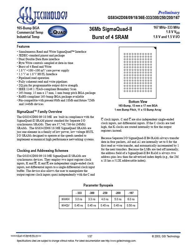
Preliminary GS8342D08/09/18/36E-333/300/250/200/167 www.DataSheet4U.com 165-Bump BGA Commercial Temp Industrial Temp Features • Simultaneous Read and Write SigmaQuad™ Int...
View more extracted text
Industrial Temp Features • Simultaneous Read and Write SigmaQuad™ Interface • JEDEC-standard pinout and package • Dual Double Data Rate interface • Byte Write controls sampled at data-in time • Burst of 4 Read and Write • 1.8 V +100/–100 mV core power supply • 1.5 V or 1.8 V HSTL Interface • Pipelined read operation • Fully coherent read and write pipelines • ZQ pin for programmable output drive strength • IEEE 1149.1 JTAG-compliant Boundary Scan • 165-bump, 15 mm x 17 mm, 1 mm bump pitch BGA package • RoHS-compliant 165-bump BGA package available • Pin-compatible with present 9Mb and 18Mb and future 72Mb and 144Mb device
 GS8342D08E-333 Datasheet