Datasheet Summary
GOFORD
N-Channel Enhancement Mode Power MOSFET
Description
The G40N03A uses advanced trench technology and design to provide excellent RDS(ON) with low gate charge. It can be used in a wide variety of applications.
General Features
- VDS =30V,ID =40A RDS(ON) <6.5mΩ @ VGS=10V RDS(ON) < 10mΩ @ VGS=4.5V
- High density cell design for ultra low Rdson
- Fully characterized avalanche voltage and current
- Good stability and uniformity with high EAS
- Excellent package for good heat dissipation
- Special process technology for high ESD capability
Application
- SMPS and general purpose applications
- Hard switched and high frequency circuits
- Uninterruptible power supply
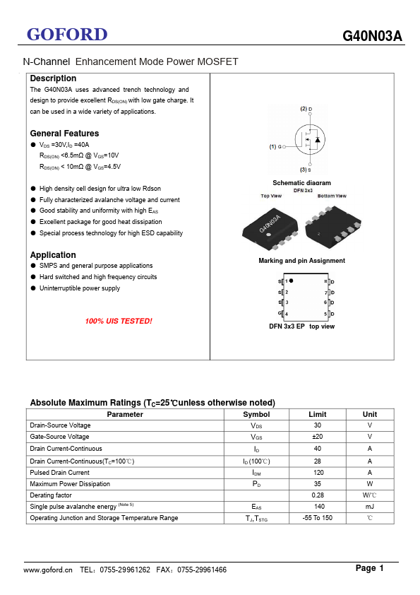
Schematic...