_ _ _ _ _ _ _ _ _ _ _ _ _ _ _ _ _ _ _ _ _ _ _ _ _ _ CMOS Peripherals
CDP1852, CDP1852C
CSI!~
MODE
OIO
000
OIl
001
OI2
002
0I3
003
CLOCK
VSS
I • 24 VOO
2 23 SR/SR
3 22 0I7
4 21 007
I.5 20 OI6
6 19 006
DI5
17 DOS
9 16 OI4
10 15 004
II I. CLEAR
12 13 CS2
TOP VIEW
92C5-27572
CDP1852, CDP1852C
TERMINAL ASSIGNMENT
Byte-Wide Input/Output Port
Features:
• Static silicon-gate CMOS circuitry
• Parallel B-bit data register and buffer
• Handshaking via service request flip-flop
• Low quiescent and operating power
• Interfaces directly with CDP1BOO-series
microprocessors
• Single voltage supply
• Full military temperature
range (-55°C to +125°C)
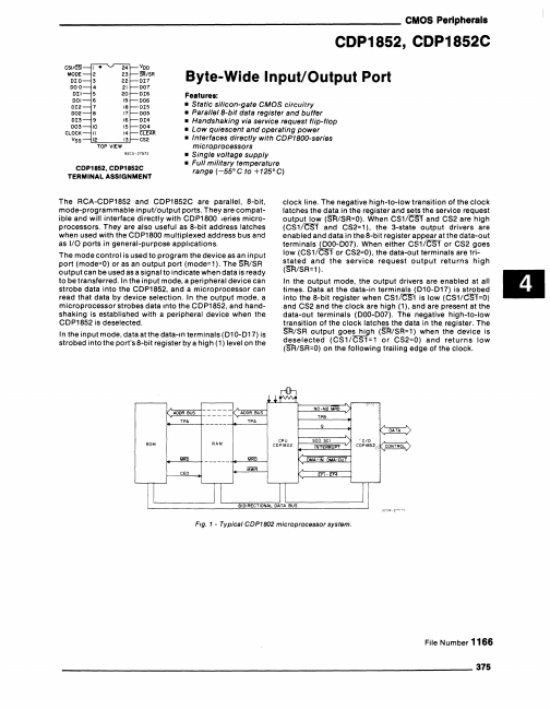
The ACA-CDP1852 and CDP1852C are parallel, 8-bit,
mode-programmable input/output ports. They are compat-
ible and will interface directly with CDP1800,eries micro-
processors. They are also useful as 8-bit address latches
when used with the CDP1800 multiplexed address bus and
as liD ports in general-purpose applications.
The mode control is used to program the device as an input
port (mode=O) or as an output port (mode=1). The Sl'!/SA
output can be used as a signal to indicate when data is ready
to be transferred. In the input mode, a peripheral device can
strobe data into the CDP1852, and a microprocessor can
read that data by device selection. In the output mode, a
microprocessor strobes data Into the CDP1852, and hand-
shaking is established with a peripheral device when the
CDP1852 is deselected.
In the input mode, data at the data-In terminals (D10-D17) is
strobed into the port's 8-bit register by a high (1) level on the
clock line. The negative high-to-Iow transition of the clock
latches the data in the register and sets the service request
output low (SR/SA=O). When CS1/CS1 and CS2 are high
(CS1/~ and CS2=1), the 3-state output drivers are
enabled and data in the8-bit register appear at the data-out
terminals (DOO-D07). When either CS1/CS1 or CS2 goes
low (CS1/CS1 or CS2=O), the data-out terminals are tri-
stated and the service request output returns high
(Sl'!/SA=1).
In the output mode, the output drivers are enabled at all
times. Data at the data-in terminals (D10-D17) is strobed
into the 8-bit register when CS1/CS1 is low (CS1/CS1=O)
and CS2 and the clock are high (1), and are present at the
data-out terminals (DOO-D07). The negative high-to-Iow
transition of the clock latches the data in the register. The
SAlSA output goes high (SR/SR=1) when the device is
deselected (CS1/CS1=1 or CS2=O) and returns low
(SR/SA=O) on the following trailing edge of the clock.
AODR BUS
TPA
----
----
-
~
ADDR BUS
TPA
NO-N2 MRO
TPB
0
I"""""'
~
~CONTROl>ROM
RAM
CPU
CDPIB02
seD SCI
INTERRUPT
'I/O
CDP18521'
MR5
MRO
OMA-IN MA-OUT
CEO
MWR
EFt EF4
[I II
Jf
BIDIRECTIONAL DATA BUS
l2:"'-?~'-'
Fig. 1 - Typical CDP1802 microprocessor system.
File Number 1166
_________________________________________________________ 375