FDMS3660AS
FDMS3660AS is MOSFET manufactured by Fairchild Semiconductor.
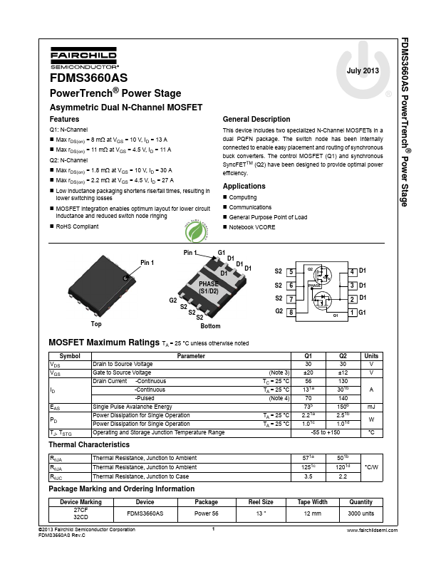
FDMS3660AS PowerTrench® Power Stage
PowerTrench® Power Stage
Asymmetric Dual N-Channel MOSFET
Features
Q1: N-Channel
- Max rDS(on) = 8 mΩ at VGS = 10 V, ID = 13 A
- Max rDS(on) = 11 mΩ at VGS = 4.5 V, ID = 11 A Q2: N-Channel
- Max rDS(on) = 1.8 mΩ at VGS = 10 V, ID = 30 A
- Max rDS(on) = 2.2 mΩ at VGS = 4.5 V, ID = 27 A
- Low inductance packaging shortens rise/fall times, resulting in lower switching losses
- MOSFET integration enables optimum layout for lower circuit inductance and reduced switch node ringing
- RoHS pliant
July 2013
General Description
This device includes two specialized N-Channel MOSFETs in a dual PQFN package. The switch node has been internally...