The following content is an automatically extracted verbatim text
from the original manufacturer datasheet and is provided for reference purposes only.
View original datasheet text
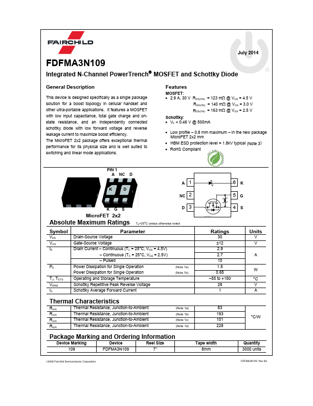
July 2014
FDFMA3N109
Integrated N-Channel PowerTrench® MOSFET and Schottky Diode
General Description
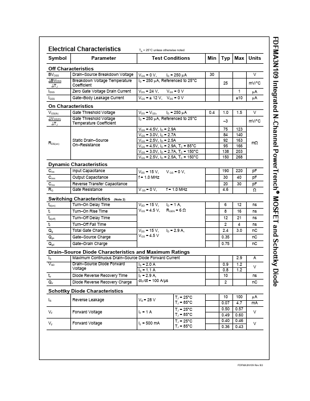
This device is designed specifically as a single package solution for a boost topology in cellular handset and other ultra-portable applications. It features a MOSFET with low input capacitance, total gate charge and onstate resistance, and an independently connected schottky diode with low forward voltage and reverse leakage current to maximize boost efficiency. The MicroFET 2x2 package offers exceptional thermal performance for its physical size and is well suited to switching and linear mode applications.
Features
MOSFET: • 2.9 A, 30 V RDS(ON) = 123 mΩ @ VGS = 4.5 V
RDS(ON) = 140 mΩ @ VGS = 3.0 V RDS(ON) = 163 mΩ @ VGS = 2.5 V
Schottky: • VF < 0.46 V @ 500mA
• Low profile – 0.
 FDFMA3N109 Datasheet