FDD3510H Overview
Key Specifications
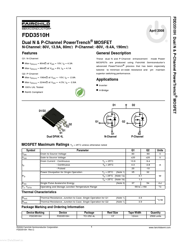
Package: TO-252
Mount Type: Surface Mount
Height: 2.517 mm
Max Operating Temp: 150 °C
Key Features
- Max rDS(on) = 80mΩ at VGS = 10V, ID = 4.3A
- Max rDS(on) = 88mΩ at VGS = 6V, ID = 4.1A Q2: P-Channel
- Max rDS(on) = 190mΩ at VGS = -10V, ID = -2.8A
- Max rDS(on) = 224mΩ at VGS = -4.5V, ID = -2.6A
- 100% UIL Tested