The following content is an automatically extracted verbatim text
from the original manufacturer datasheet and is provided for reference purposes only.
View original datasheet text
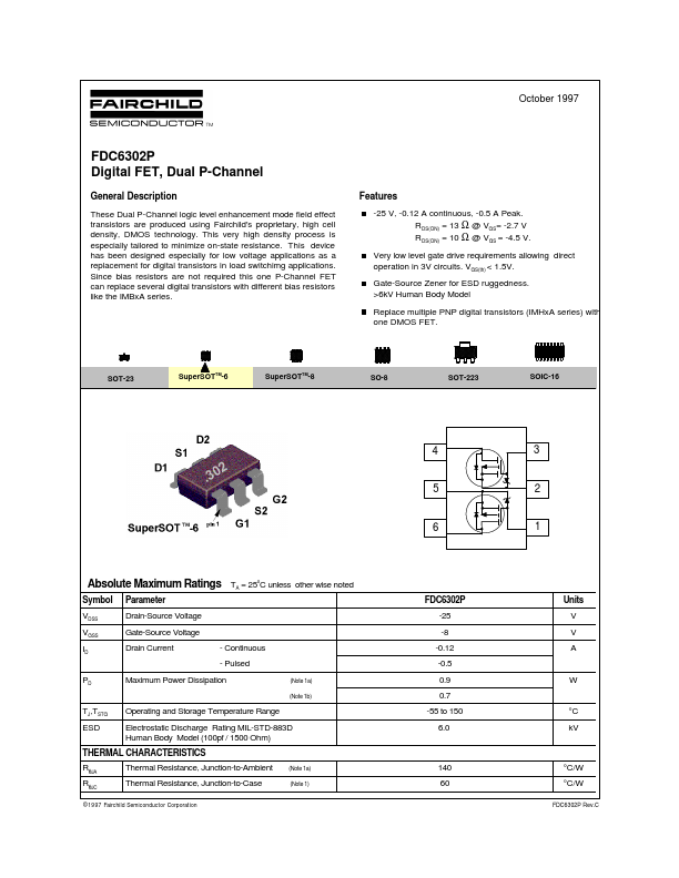
October 1997
FDC6302P Digital FET, Dual P-Channel
General Description
These Dual P-Channel logic level enhancement mode field effect transistors are produced using Fairchild's proprietary, high cell density, DMOS technology. This very high density process is especially tailored to minimize on-state resistance. This device has been designed especially for low voltage applications as a replacement for digital transistors in load switchimg applications. Since bias resistors are not required this one P-Channel FET can replace several digital transistors with different bias resistors like the IMBxA series.
Features
-25 V, -0.12 A continuous, -0.5 A Peak. R DS(ON) = 13 Ω @ VGS= -2.7 V R DS(ON) = 10 Ω @ VGS = -4.5 V.
 FDC6302P Datasheet