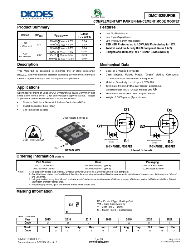
General Description
Key Features
Full PDF Text Transcription for DMC1028UFDB (Reference)
Note: Below is a high-fidelity text extraction (approx. 800 characters) for
DMC1028UFDB . For precise diagrams, and layout, please refer to the original PDF.
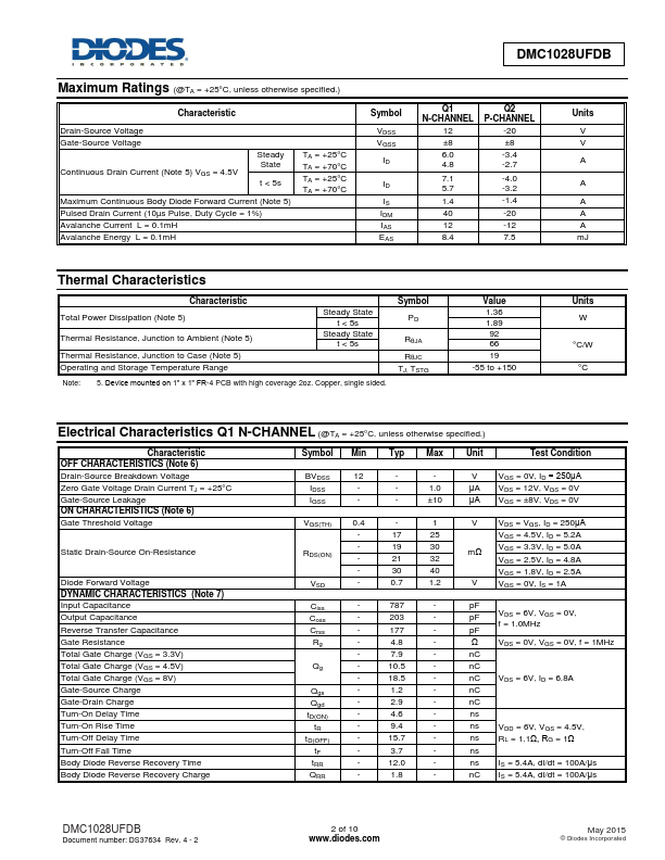
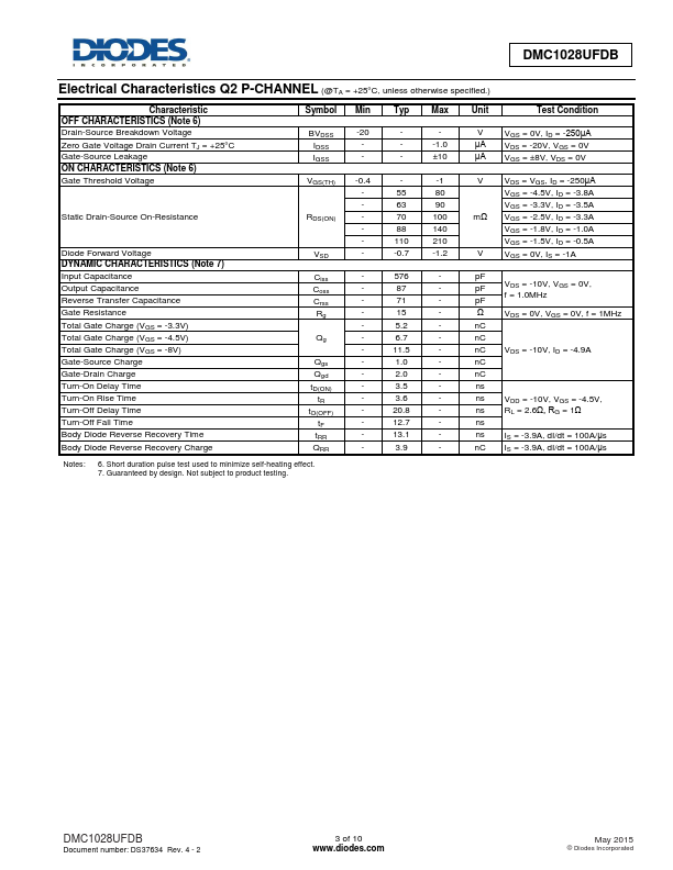
DMC1028UFDB Product Summary COMPLEMENTARY PAIR ENHANCEMENT MODE MOSFET Features Device BVDSS Q1 N-Channel 12V Q2 P-Channel -20V Description RDS(ON) max 25mΩ @ VGS = 4.5V ...
View more extracted text
annel 12V Q2 P-Channel -20V Description RDS(ON) max 25mΩ @ VGS = 4.5V 30mΩ @ VGS = 3.3V 32mΩ @ VGS = 2.5V 80mΩ @ VGS = -4.5V 90mΩ @ VGS = -3.3V 100mΩ @ VGS = -2.5V ID max TA = +25°C 6.0A 5.5A 5.3A -3.4A -3.2A -3.0A Low On-Resistance Low Input Capacitance Low Profile, 0.6mm Max Height ESD HBM Protected up to 1.5KV, MM Protected up to 150V. Totally Lead-Free & Fully RoHS Compliant (Notes 1 & 2) Halogen and Antimony Free. “Green” Device (Note 3) Mechanical Data This MOSFET is designed to minimize the on-state resistance (RDS(ON)) and yet maintain superior switching performance, making it ideal for high-efficiency
More Datasheets from Diodes Incorporated
 DMC1028UFDB Datasheet