CY7C198
CY7C198 is 32K x 8 Static RAM manufactured by Cypress.
- Part of the CY7 comparator family.
- Part of the CY7 comparator family.
Features
D D D D D D D
High speed Ċ 15 ns CMOS for optimum speed/power Low active power Ċ 990 m W Low standby power Ċ 195 m W Easy memory expansion with CE and OE features
TTLĆpatible inputs and outputs Automatic powerĆdown when deselected
The CY7C198 is a highĆperformance CMOS static RAM organized as 32,768 words by8bits.Easymemoryexpansionis provided by an active LOW chip enable (CE)andactive LOWoutputenable(OE) and threeĆstate drivers. This device has an automatic powerĆdown feature
, reducing the power consumption by 80% when deĆ selected. The CY7C198 is available in a 600ĆmilĆwide cer DIP and LCC package and a 32Ćlead TSOP package. An active LOW write enable signal (WE) controls the writing/reading operation of the memory. When CE and WE inputs areboth LOW,dataontheeightdatainput/
Functional Description output pins (I/O0 through I/O7) is written intothememorylocationaddressedbythe address present on the address pins (A0 through A14). Reading the device is acĆ plishedbyselectingthedeviceandenĆ abling the outputs, CE and OE active LOW, while WE remains inactive or HIGH. Under these conditions, the conĆ tents of the location addressed by the inĆ formationonaddresspinsispresentonthe eight data input/output pins. Theinput/outputpinsremaininahighĆimĆ pedance state unless the chip is selected, outputs are enabled, and write enable (WE) is HIGH. A die coat is used to ensure alpha immunity.
32K x 8 Static RAM
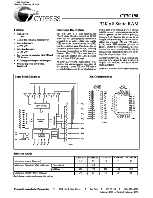
Logic Block Diagram
Pin Configurations
Cer DIP Top View
A5 A6 A7 A8 A9 A10 I/O0 A11 A12 I/O1 A13 A14 1 2 3 4 5 6 7 8 9 10 11 12 13 14 28 27 26 25 24 23 22 21 20 19 18 17 16 15 VCC WE A4 A3 A2 A1 OE A0 CE I/O7 I/O6 I/O5 I/O4 I/O3 A6 A5 A4 A3 A2 A1 A0 NC I/O0 4 5 6 7 8 9 10 11 12 13 A7 A 12 A 14 V CC
LCC Top View
3 2 1 32 31 30 29 28 27 26 25 24 23 22 21 A8 A9 A11 NC OE A10 CE I/O7 I/O6 WE NC A 13 C198Ć1
INPUT BUFFER
A0
ROW DECODER
A1 A2 A3 A4 A5 A6 A7 A8 A9
I/O0 I/O2 SENSE AMPS I/O1 I/O2 I/O3 GND
14 15 16 17 1819 20 GND I/O 1 I/O 2 NC I/O 3 I/O 4 I/O...