Datasheet4U Logo Datasheet4U.com

CY7C1356B - 9-Mb (256K x 36/512K x 18) Pipelined SRAM

General Description

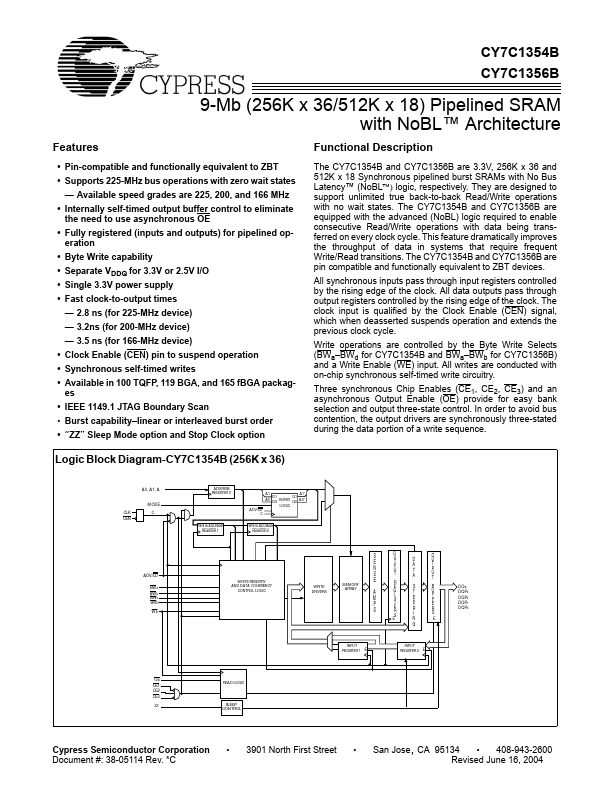
The CY7C1354B and CY7C1356B are 3.3V, 256K x 3

Key Features

  • Pin-compatible and functionally equivalent to ZBT.
  • Supports 225-MHz bus operations with zero wait states.
  • Available speed grades are 225, 200, and 166 MHz.
  • Internally self-timed output buffer control to eliminate the need to use asynchronous OE.
  • Fully registered (inputs and outputs) for pipelined op- eration.
  • Byte Write capability.
  • Separate VDDQ for 3.3V or 2.5V I/O.
  • Single 3.3V power supply.
  • Fast clock-to-output t.

📥 Download Datasheet

Full PDF Text Transcription (Reference)

The following content is an automatically extracted verbatim text from the original manufacturer datasheet and is provided for reference purposes only.

View original datasheet text
CY7C1354B CY7C1356B 9-Mb (256K x 36/512K x 18) Pipelined SRAM with NoBL™ Architecture Features • Pin-compatible and functionally equivalent to ZBT • Supports 225-MHz bus operations with zero wait states — Available speed grades are 225, 200, and 166 MHz • Internally self-timed output buffer control to eliminate the need to use asynchronous OE • Fully registered (inputs and outputs) for pipelined op- eration • Byte Write capability • Separate VDDQ for 3.3V or 2.5V I/O • Single 3.3V power supply • Fast clock-to-output times — 2.8 ns (for 225-MHz device) — 3.2ns (for 200-MHz device) — 3.5 ns (for 166-MHz device) • Clock Enable (CEN) pin to suspend operation • Synchronous self-timed writes • Available in 100 TQFP, 119 BGA, and 165 fBGA packages • IEEE 1149.