Datasheet Details
| Part number | CY7C1352G |
|---|---|
| Manufacturer | Cypress (Infineon) |
| File Size | 824.13 KB |
| Description | 4-Mbit (256K x 18) Pipelined SRAM |
| Datasheet |
 CY7C1352G Datasheet CY7C1352G Datasheet
|
|
|
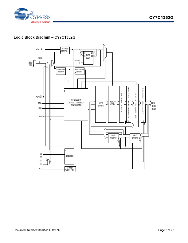
The CY7C1352G is a 3.3 V, 256K × 18 synchronous-pipelined burst SRAM designed specifically to support unlimited true back-to-back read/write operations without the insertion of wait states.
| Part number | CY7C1352G |
|---|---|
| Manufacturer | Cypress (Infineon) |
| File Size | 824.13 KB |
| Description | 4-Mbit (256K x 18) Pipelined SRAM |
| Datasheet |
CY7C1352G Datasheet
|
|
|
|
| Part Number | Description | Manufacturer |
|---|---|---|
| CY7C131AE | 1K/2K x 8 Dual-Port Static RAM | Cypress |
| CY7C131E | 1K/2K x 8 Dual-Port Static RAM | Cypress |
| CY7C136AE | 1K/2K x 8 Dual-Port Static RAM | Cypress |
| CY7C136E | 1K/2K x 8 Dual-Port Static RAM | Cypress |
| CY7C1370C | 512K x 36/1M x 18 Pipelined SRAM with NoBL Architecture | Cypress |
| Part Number | Description |
|---|---|
| CY7C1352 | 256K x18 Pipelined SRAM |
| CY7C1352F | 4-Mbit (256K x 18) Pipelined SRAM |
| CY7C135 | 4K x 8 Dual-Port Static RAM and 4K x 8 Dual-Port SRAM |
| CY7C1350G | 4-Mbit (128K x 36) Pipelined SRAM |
| CY7C1351 | 128Kx36 Flow-Through SRAM |
The following content is an automatically extracted verbatim text from the original manufacturer datasheet and is provided for reference purposes only.