CY29942
Overview
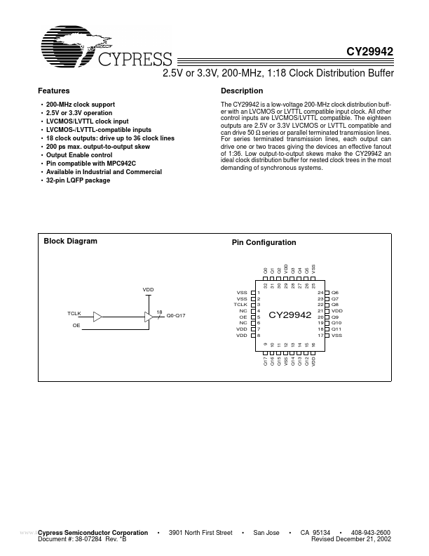
The CY29942 is a low-voltage 200-MHz clock distribution buffer with an LVCMOS or LVTTL compatible input clock. All other control inputs are LVCMOS/LVTTL compatible.
- 200-MHz clock support 2.5V or 3.3V operation LVCMOS/LVTTL clock input LVCMOS-/LVTTL-compatible inputs 18 clock outputs: drive up to 36 clock lines 200 ps max. output-to-output skew Output Enable control Pin compatible with MPC942C Available in Industrial and Commercial 32-pin LQFP package