Click to expand full text
47
CY29947
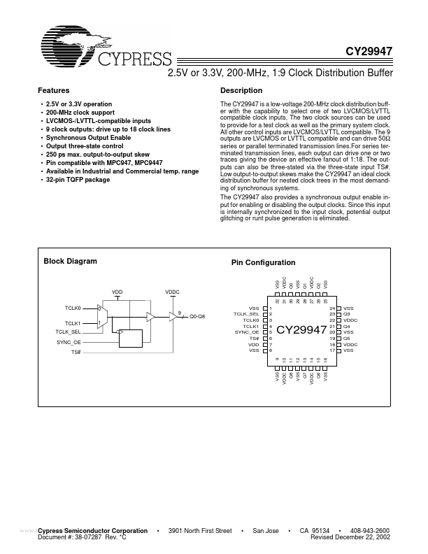
2.5V or 3.3V, 200-MHz, 1:9 Clock Distribution Buffer
Features
• • • • • • • • • • 2.5V or 3.3V operation 200-MHz clock support LVCMOS-/LVTTL-compatible inputs 9 clock outputs: drive up to 18 clock lines Synchronous Output Enable Output three-state control 250 ps max. output-to-output skew Pin compatible with MPC947, MPC9447 Available in Industrial and Commercial temp. range 32-pin TQFP package
Description
The CY29947 is a low-voltage 200-MHz clock distribution buffer with the capability to select one of two LVCMOS/LVTTL compatible clock inputs. The two clock sources can be used to provide for a test clock as well as the primary system clock. All other control inputs are LVCMOS/LVTTL compatible.
 CY29947 Datasheet