CY29351
CY29351 is 9-Output Zero Delay manufactured by Cypress.
PRELIMINARY CY29351
2.5V or 3.3V, 200 MHz, 9-Output Zero Delay
Features
- -
- -
Functional Description
The CY29351 is a low voltage high performance 200 MHz PLL-based zero delay buffer designed for high speed clock distribution applications. The CY29351 Features
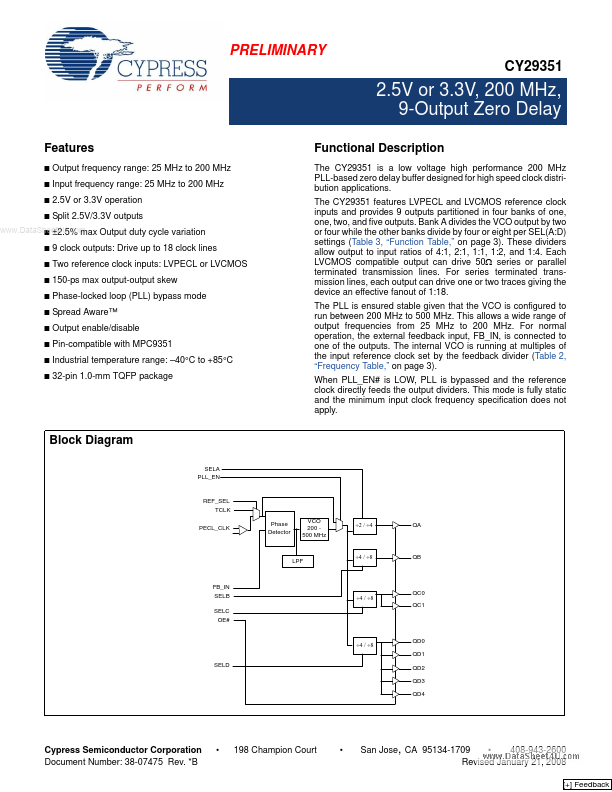
LVPECL and LVCMOS reference clock inputs and provides 9 outputs partitioned in four banks of one, one, two, and five outputs. Bank A divides the VCO output by two or four while the other banks divide by four or eight per SEL(A:D) settings (Table 3, “Function Table,” on page 3). These dividers allow output to input ratios of 4:1, 2:1, 1:1, 1:2, and 1:4. Each LVCMOS patible output can drive 50Ω series or parallel terminated transmission lines. For series terminated transmission lines, each output can drive one or two traces giving the device an effective fanout of 1:18. The PLL is ensured stable given that the VCO is configured to run between 200 MHz to 500 MHz. This allows a wide range of output frequencies from 25 MHz to 200 MHz. For normal operation, the external feedback input, FB_IN, is connected to one of the outputs. The internal VCO is running at multiples of the input reference clock set by the feedback divider (Table 2, “Frequency Table,” on page 3). When PLL_EN# is LOW, PLL is bypassed and the reference clock directly feeds the output dividers. This mode is fully static and the minimum input clock frequency specification does not apply.
Output frequency range: 25 MHz to 200 MHz Input frequency range: 25 MHz to 200 MHz 2.5V or 3.3V operation Split 2.5V/3.3V outputs
..
- ±2.5% max Output duty cycle variation
- -
- -
- -
- -
- 9 clock outputs: Drive up to 18 clock lines Two reference clock inputs: LVPECL or LVCMOS 150-ps max output-output skew Phase-locked loop (PLL) bypass mode Spread Aware™ Output enable/disable Pin-patible with MPC9351 Industrial temperature range:
- 40°C to +85°C 32-pin 1.0-mm TQFP package
Block Diagram
SELA PLL_EN
REF_SEL TCLK PECL_CLK Phase Detector...