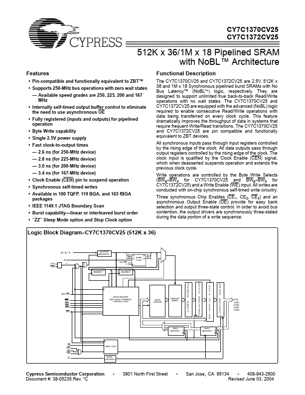
CY7C1372CV25
Features
- Pin-patible and functionally equivalent to ZBT™
- Supports 250-MHz bus operations with zero wait states
- Available speed grades are 250, 225, 200 and 167 MHz
- Internally self-timed output buffer control to eliminate the need to use asynchronous OE
- Fully registered (inputs and outputs) for pipelined operation
- Byte Write capability
- Single 2.5V power supply
- Fast clock-to-output times
- 2.6 ns (for 250-MHz device)
- 2.8 ns (for 225-MHz device)
- 3.0 ns (for 200-MHz device)
- 3.4 ns (for 167-MHz device)
- Clock Enable (CEN) pin to suspend operation
- Synchronous self-timed writes
- Available in 100 TQFP, 119 BGA, and 165 f BGA packages
- IEEE 1149.1 JTAG Boundary Scan
- Burst capability- linear or interleaved burst order
- “ZZ” Sleep Mode option and Stop Clock option
Functional Description
The CY7C1370CV25 and CY7C1372CV25 are 2.5V, 512K x 36 and 1M x 18 Synchronous pipelined burst SRAMs with No Bus Latency™ (No BL) logic, respectively. They are designed to support...