CY7C131E
Features
- True dual-ported memory cells, which allow simultaneous reads of the same memory location
- 1K/2K × 8 organization
- 0.35 micron plementary metal oxide semiconductor
(CMOS) for optimum speed and power
- High speed access: 15 ns
- Low operating power: ICC = 110 m A (typical),
Standby: ISB3 = 0.05 m A (typical)
- Fully asynchronous operation
- Automatic power-down
- BUSY output flag to indicate access to the same location by both ports
- INT flag for port-to-port munication
- Available in 52-pin plastic leaded chip carrier (PLCC), 52-pin plastic quad flat package (PQFP)
- Pb-free packages available
Functional Description
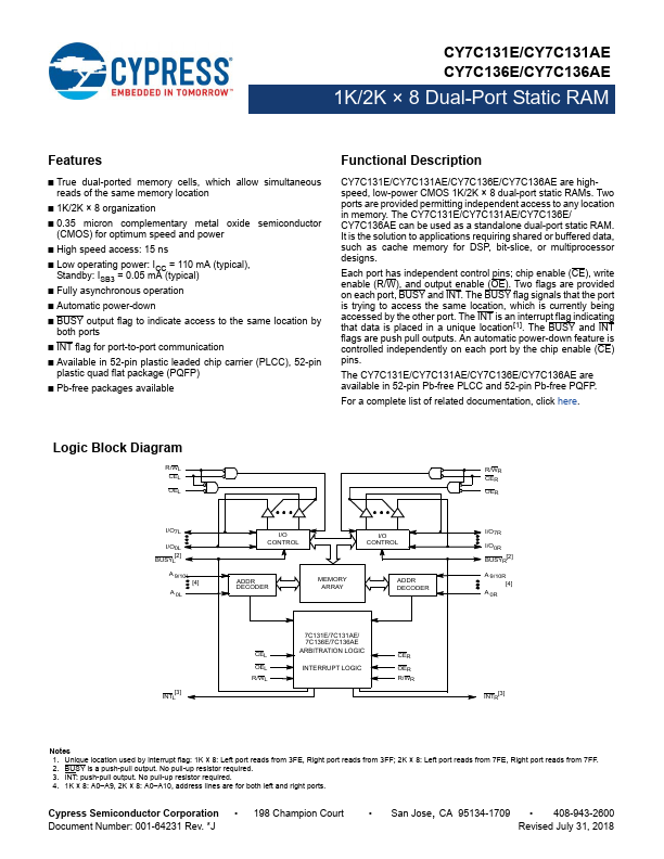
CY7C131E/CY7C131AE/CY7C136E/CY7C136AE are highspeed, low-power CMOS 1K/2K × 8 dual-port static RAMs. Two ports are provided permitting independent access to any location in memory. The CY7C131E/CY7C131AE/CY7C136E/ CY7C136AE can...