CGH31240F Description
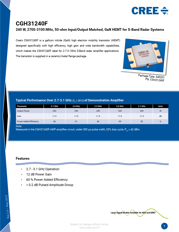
CGH31240F 240 W, 2700-3100 MHz, 50-ohm Input/Output Matched, GaN HEMT for S-Band Radar Systems Cree’s CGH31240F is a gallium nitride (GaN) high electron mobility transistor (HEMT) designed specifically with high efficiency, high gain and wide bandwidth capabilities, which makes the CGH31240F ideal for 2.7-3.1GHz S-Band radar amplifier applications. The transistor is supplied in a ceramic/metal flange package....
CGH31240F Key Features
- 3.1 GHz Operation
- 12 dB Power Gain
- 60 % Power Added Efficiency
- < 0.2 dB Pulsed Amplitude Droop
- May 2015