CEU65P03
CEU65P03 is P-Channel MOSFET manufactured by CET.
CED65P03/CEU65P03
P-Channel Enhancement Mode Field Effect Transistor
Features
-30V, -65A, RDS(ON) = 9mΩ @VGS = -10V. RDS(ON) = 12mΩ @VGS = -4.5V.
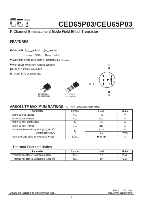
Super high dense cell design for extremely low RDS(ON). High power and current handing capability. Lead free product is acquired. TO-251 & TO-252 package.
CEU SERIES TO-252(D-PAK)
G DS
CED SERIES...