FEATURES
nn AEC-Q100 Qualified for Automotive Applications
nn Silent Switcher®2 Architecture for Low EMI
nn VIN Range: 3.1V to 20V
nn VOUT Range: 0.6V to 5.5V
nn Differential VOUT Remote Sense
nn Adjustable Frequency: 400kHz to 3MHz
nn PolyPhase® Operation: Up to 12 Phases
nn Output Tracking and Soft-Start
nn Reference Accuracy: 0.6V ±1% Over Temperature
nn Current Mode Operation for Excellent Line and Load
Transient Response
nn Accurate 1.2V Run Pin Threshold
nn Supports Forced Continuous/Discontinuous Modes
nn 42-Lead 6mm × 5mm × 1.3mm BGA Package
APPLICATIONS
nn Server Power Applications
nn Distributed Power Systems
nn Point of Load Supply for ASIC, FPGA, DSP, µP, etc.
All registered trademarks and trademarks are the property of their respective owners.
LTC7150S/LTC7150S-4
20V, 20A Synchronous
Step-Down Regulator
DESCRIPTION
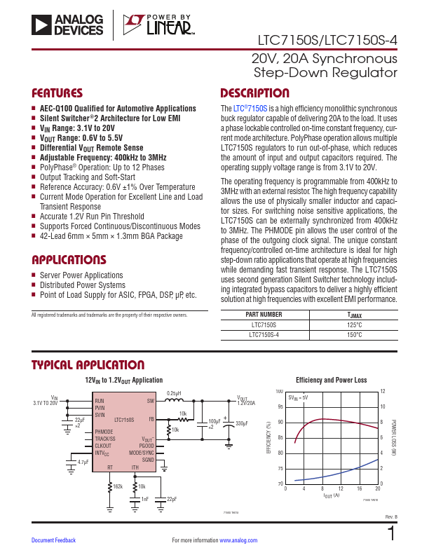
The LTC®7150S is a high efficiency monolithic synchronous
buck regulator capable of delivering 20A to the load. It uses
a phase lockable controlled on-time constant frequency, cur-
rent mode architecture. PolyPhase operation allows multiple
LTC7150S regulators to run out-of-phase, which reduces
the amount of input and output capacitors required. The
operating supply voltage range is from 3.1V to 20V.
The operating frequency is programmable from 400kHz to
3MHz with an external resistor. The high frequency capability
allows the use of physically smaller inductor and capaci-
tor sizes. For switching noise sensitive applications, the
LTC7150S can be externally synchronized from 400kHz
to 3MHz. The PHMODE pin allows the user control of the
phase of the outgoing clock signal. The unique constant
frequency/controlled on-time architecture is ideal for high
step-down ratio applications that operate at high frequencies
while demanding fast transient response. The LTC7150S
uses second generation Silent Switcher technology includ-
ing integrated bypass capacitors to deliver a highly efficient
solution at high frequencies with excellent EMI performance.
PART NUMBER
LTC7150S
LTC7150S-4
TJMAX
125°C
150°C
TYPICAL APPLICATION
VIN
3.1V TO 20V
12VIN to 1.2VOUT Application
22µF
×2
4.7µF
RUN
PVIN
SVIN
LTC7150S
SW
FB
PHMODE
TRACK/SS
CLKOUT
INTVCC
RT
VOUT–
PGOOD
MODE/SYNC
SGND
ITH
0.25µH
10k
10k
162k
10k
1nF
22pF
100µF +
×2
VOUT
1.2V/20A
330µF
7150S TA01a
Document Feedback
For more information www.analog.com
Efficiency and Power Loss
100
SVIN = 5V
95
12
10
90 8
85 6
80 4
75 2
70 0
0 4 8 12 16 20
IOUT (A)
7150S TA01b
Rev. B
1