HMC1118
Overview
Data Sheet
Online Documentation
Design Resources
Discussion
Sample & Buy
High Isolation, Silicon SPDT,
Nonrefective Switch, 9 k Hz to 13.0 GHz
FEATURES
Nonreflective 50 Ω design Positive control: 0 V/3.3 V Low insertion loss: 0.68 d B at 8.0 GHz High isolation: 48 d B at 8.0 GHz High power handling
35 d Bm through path 27 d Bm terminated path High linearity 1 d B pression (P1d B): 37 d Bm typical Input third-order intercept (IIP3): 62 d Bm typical ESD rating: 2 k V human body model (HBM) 3 mm × 3 mm, 16-lead LFCSP package No low frequency spurious Settling time (0.05 d B margin of final RFOUT): 7.5 μs
APPLICATIONS
Test instrumentation Microwave radios and very small aperture terminals (VSATs) Military radios, radars, and electronic counter measures (ECMs) Fiber optics and broadband telemunications
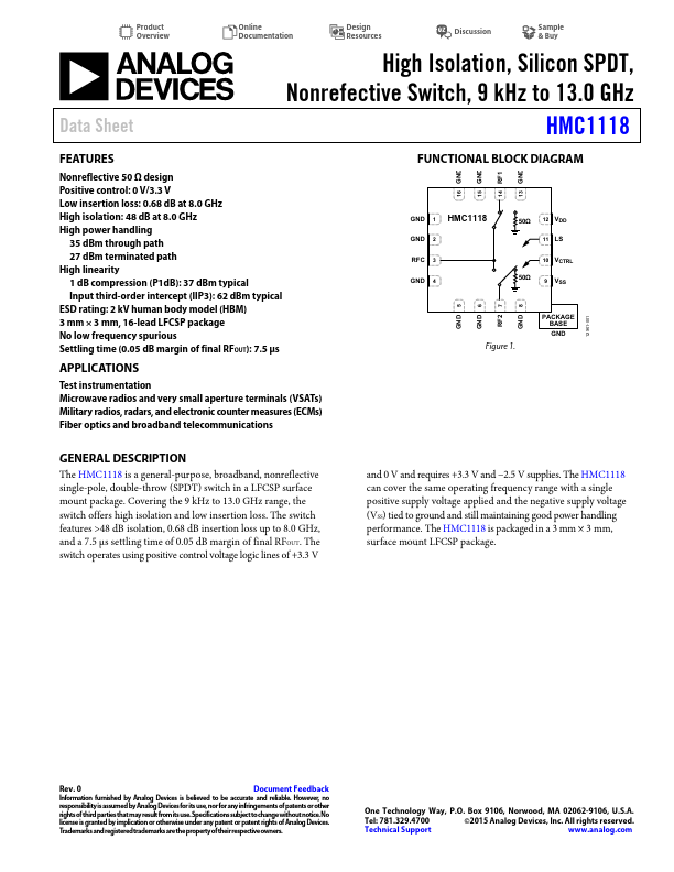
FUNCTIONAL BLOCK DIAGRAM
16 GND 15 GND 14 RF1 13 GND
GND 1 HMC1118
GND 2 RFC 3 GND 4
50Ω 12 VDD 11 LS
50Ω
10 VCTRL 9 VSS
Figure 1.
PACKAGE BASE GND
GND 5 GND 6 RF2 7...