Datasheet Details
| Part number | ADN2818 |
|---|---|
| Manufacturer | Analog Devices |
| File Size | 343.29 KB |
| Description | (ADN2817 / ADN2818) Clock and Data Recovery IC |
| Datasheet |
 ADN2818 Datasheet ADN2818 Datasheet
|
|
|
Download the ADN2818 datasheet PDF. This datasheet also covers the ADN2817 variant, as both devices belong to the same (adn2817 / adn2818) clock and data recovery ic family and are provided as variant models within a single manufacturer datasheet.
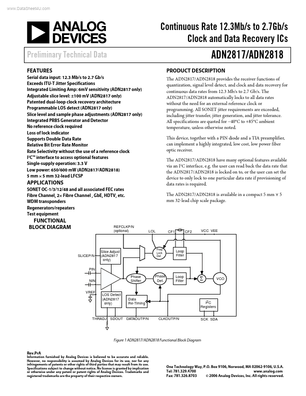
The ADN2817/ADN2818 provides the receiver functions of quantization, signal level detect, and clock and data recovery for continuous data rates from 12.3 Mb/s to 2.7 Gb/s.
The ADN2817/ADN2818 automatically locks to all data rates without the need for an external reference clock or programming.
| Part number | ADN2818 |
|---|---|
| Manufacturer | Analog Devices |
| File Size | 343.29 KB |
| Description | (ADN2817 / ADN2818) Clock and Data Recovery IC |
| Datasheet |
ADN2818 Datasheet
|
|
|
|
| Part Number | Description | Manufacturer |
|---|---|---|
| ADN2.5-24-1PM | AC-DC / DIN Rail Mount | Emerson |
| ADN20-24-1PM | AC-DC / DIN Rail Mount | Emerson |
| ADN20-24-3PM | AC-DC / DIN Rail Mount | Emerson |
| ADN003 | Select the Right Operational Amplifier | MicroChip |
| ADN1-48-1PP | AC-DC / DIN Rail Mount | Emerson |
| Part Number | Description |
|---|---|
| ADN2811 | OC-48/OC-48 FEC Clock and Data Recovery IC |
| ADN2812 | Continuous Rate 12.3 Mb/s to 2.7 Gb/s Clock and Data Recovery IC with Integrated Limiting Amp |
| ADN2813 | Clock and Data Recovery IC |
| ADN2814 | Continuous Rate 10 Mb/s to 675 Mb/s Clock and Data Recovery |
| ADN2815 | Clock and Data Recovery IC |
The following content is an automatically extracted verbatim text from the original manufacturer datasheet and is provided for reference purposes only.