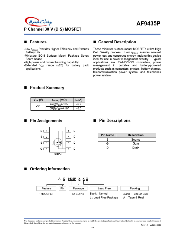
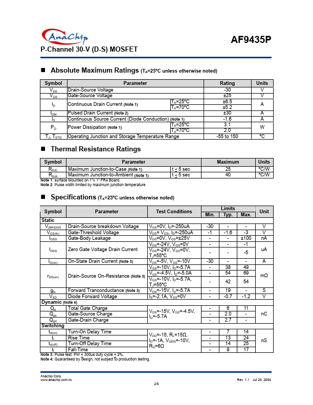
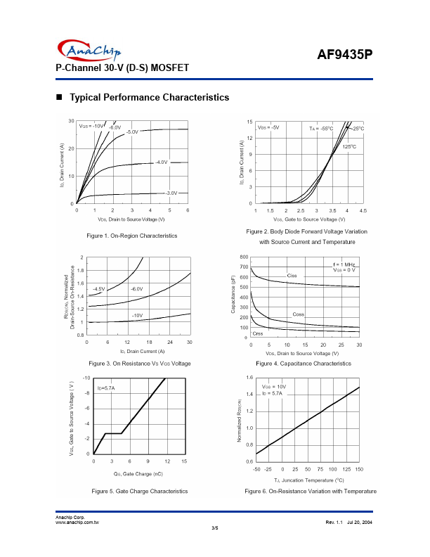
P-Channel 30-V (D-S) MOSFET
AF9435P
Absolute Maximum Ratings (TA=25ºC unless otherwise noted)
Symbol
VDS
VGS
ID
IDM
IS
PD
TJ, TSTG
Parameter
Drain-Source Voltage
Gate-Source Voltage
Continuous Drain Current (Note 1)
Pulsed Drain Current (Note 2)
TA=25ºC
TA=70ºC
Continuous Source Current (Diode Conduction) (Note 1)
Power Dissipation (Note 1)
TA=25ºC
TA=70ºC
Operating Junction and Storage Temperature Range
Rating
-30
±25
±6.5
±5.2
±30
-1.6
3.1
2.0
-55 to 150
Thermal Resistance Ratings
Units
V
V
A
A
A
W
ºC
Symbol
Parameter
RθJC Maximum Junction-to-Case (Note 1)
RθJA Maximum Junction-to-Ambient (Note 1)
Note 1: surface Mounted on 1”x 1” FR4 Board.
Note 2: Pulse width limited by maximum junction temperature
t < 5 sec
t < 5 sec
Specifications (TA=25ºC unless otherwise noted)
Symbol
Parameter
Test Conditions
Static
V(BR)DSS
VGS(th)
IGSS
Drain-Source breakdown Voltage
Gate-Threshold Voltage
Gate-Body Leakage
IDSS Zero Gate Voltage Drain Current
ID(on)
On-State Drain Current (Note 3)
rDS(on) Drain-Source On-Resistance (Note 3)
gfs Forward Tranconductance (Note 3)
VSD Diode Forward Voltage
Dynamic (Note 4)
VGS=0V, ID=-250uA
VDS= VGS, ID=-250uA
VDS=0V, VGS=±25V
VDS=-24V, VGS=0V
VDS=-24V, VGS=0V,
TJ=55ºC
VDS=-5V, VGS=-10V
VGS=-10V, ID=-5.7A
VGS=-4.5V, ID=-5.0A
VGS=-10V, ID=-5.7A,
TJ=55ºC
VDS=-15V, ID=-5.7A
IS=-2.1A, VGS=0V
Qg Total Gate Charge
Qgs Gate-Source Charge
Qgd Gate-Drain Charge
Switching
VDS=-15V, VGS=-4.5V,
ID=-5.7A
td(on)
Turn-On Delay Time
tr Rise Time
td(off)
Turn-Off Delay Time
tf Fall-Time
Note 3: Pulse test: PW < 300us duty cycle < 2%.
VDD=-15, RL=15Ω,
ID=-1A, VGEN=-10V,
RG=6Ω
Note 4: Guaranteed by design, not subject to production testing.
Maximum
25
40
Units
ºC/W
ºC/W
Limits
Min. Typ. Max.
Unit
-30 - - V
-1 -1.6 -3
V
- - ±100 nA
- - -1
- - -5 uA
-30 - - A
- 38 49
- 54 69 mΩ
- 42 54
- 19 -
S
-
-0.7 -1.2
V
- 6 11
- 2.0 - nC
- 2.7 -
- 7 14
-
-
13
14
24
25
nS
- 9 17
Anachip Corp.
www.anachip.com.tw
Rev. 1.1 Jul 20, 2004
2/5