AS7C1026C Overview
Key Specifications
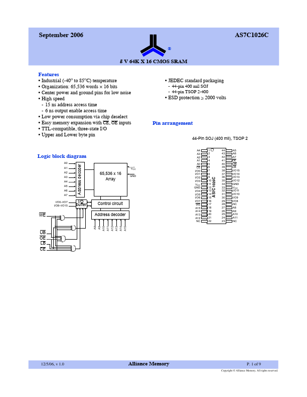
Pins: 44
Operating Voltage: 5 V
Max Voltage (typical range): 5.5 V
Min Voltage (typical range): 4.5 V
Key Features
- JEDEC standard packaging
- ESD protection > _ 2000 volts
- 44-pin 400 mil SOJ
| Part | AS7C1026C |
|---|---|
| Description | 5V 64K x 16 CMOS SRAM |
| Manufacturer | Alliance Semiconductor |
| Size | 287.41 KB |
Pins: 44
Operating Voltage: 5 V
Max Voltage (typical range): 5.5 V
Min Voltage (typical range): 4.5 V
| Seller | Inventory | Price Breaks | Buy |
|---|---|---|---|
| Newark | 0 | 160+ : 8.47 USD 250+ : 7.06 USD 500+ : 6.86 USD |
View Offer |
| Mouser | 29 | 1+ : 10.13 USD 10+ : 9.42 USD 50+ : 8.9 USD 100+ : 8.9 USD |
View Offer |
| Part Number | Manufacturer | Description |
|---|---|---|
| AS7C1025B | Alliance Semiconductor Corporation | 5V 128K x 8 CMOS SRAM |
| AS7C1024B | Alliance Semiconductor Corporation | 5V 1Mb FAST Asynchronous SRAM |