Datasheet4U Logo Datasheet4U.com

AS4C64M16D1 - 64M x 16 bit DDR1 Synchronous DRAM

Datasheet Summary

Description

The AS4C64M16D1 is a four bank DDR DRAM organized as 4 banks x 16Mbit x 16.

The AS4C64M16D1 achieves high speed data transfer rates by employing a chip architecture that prefetches multiple bits and then synchronizes the output data to a system clock.

Features

  • High speed data transfer rates with system frequency up to 200MHz - Data Mask for Write Control - Four Banks controlled by BA0 & BA1 - Programmable CAS Latency: 2, 2.5, 3 - Programmable Wrap Sequence: Sequential or Interleave - Programmable Burst Length: 2, 4, 8 for Sequential Type 2, 4, 8 for Interleave Type - Automatic and Controlled Precharge Command - Power Down Mode - Auto Refresh and Self Refresh - Refresh Interval: 8192 cycles/64 ms - 
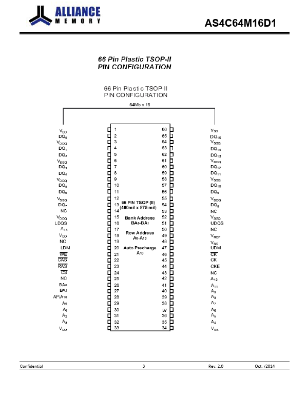
Available in 66 Pin TSOP II - SSTL-2 Compatible I/Os -.

📥 Download Datasheet

Datasheet preview – AS4C64M16D1

Datasheet Details

Part number AS4C64M16D1
Manufacturer Alliance Semiconductor
File Size 5.57 MB
Description 64M x 16 bit DDR1 Synchronous DRAM
Datasheet download datasheet AS4C64M16D1 Datasheet
Additional preview pages of the AS4C64M16D1 datasheet.
Other Datasheets by Alliance Semiconductor

Full PDF Text Transcription

Click to expand full text
AS4C64M16D1 Revision History AS4C64M16D1 – 66-pin TSOP II package Revision Rev 1.0 Rev 2 Details Preliminary datasheet Speed grade option changed -5(400MHz) to -6(333MHz) Date Sep 2014 Oct 2014 Confidential 1 Rev. 2.0 Oct. /2014 AS4C64M16D1 Confidential 64M x 16 bit DDR1 Synchronous DRAM (SDRAM) Advanced (Rev. 2.0, Oct. /2014) Features High speed data transfer rates with system frequency up to 200MHz - Data Mask for Write Control - Four Banks controlled by BA0 & BA1 - Programmable CAS Latency: 2, 2.
Published: |