Datasheet4U Logo Datasheet4U.com

QPB9325 - High Power Switch LNA Module

Description

2500 pcs on a 13” reel Evaluation board Datasheet, March 29, 2019 | Subject to change without notice 1 of 12 www.qorvo.com QPB9325 ® High Power Switch LNA Module Absolute Maximum Ratings Recommended Operating Conditions Parameter Rating Storage Temperature -50 to +150 °C Max Operating T

Features

  • 3.6-3.8 GHz frequency range.
  • Integrates a high power switch, two LNA stages, pin diode driver circuits, and dc converter.
  • Ideal for TDD systems with an isolator.
  • Only requires a 5 V supply with 3.3 V logic Ctrl.
  • Max RF Input power: 52 W Pavg (8 dB PAR).
  • 34.1 dB gain.
  • 1.2 dB noise figure.
  • -2.2 dBm IIP3 (Rx mode).
  • 0.5 dB Insertion Loss (Tx mode).
  • Compact package size, 8x8 mm 16 TERM 15 NC 14 NC 13 NC Pin.

📥 Download Datasheet

Datasheet Details

Part number QPB9325
Manufacturer qorvo
File Size 1.65 MB
Description High Power Switch LNA Module
Datasheet download datasheet QPB9325 Datasheet

Full PDF Text Transcription

Click to expand full text
QPB9325 ® High Power Switch LNA Module Product Overview 
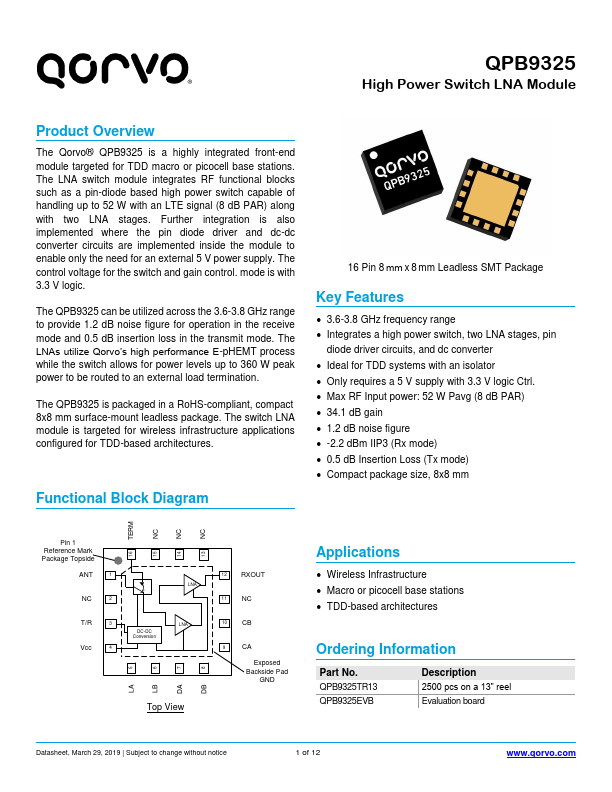
The Qorvo® QPB9325 is a highly integrated front-end module targeted for TDD macro or picocell base stations. The LNA switch module integrates RF functional blocks such as a pin-diode based high power switch capable of handling up to 52 W with an LTE signal (8 dB PAR) along with two LNA stages. Further integration is also implemented where the pin diode driver and dc-dc converter circuits are implemented inside the module to enable only the need for an external 5 V power supply. The control voltage for the switch and gain control. mode is with 3.3 V logic. The QPB9325 can be utilized across the 3.6-3.8 GHz range to provide 1.2 dB noise figure for operation in the receive mode and 0.5 dB insertion loss in the transmit mode.
Published: |