Click to expand full text
74LVC595A
8-bit serial-in/serial-out or parallel-out shift register; 3-state
Rev. 3 — 19 November 2021
Product data sheet
1. General description
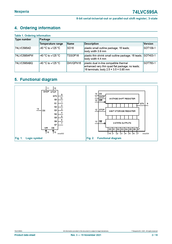
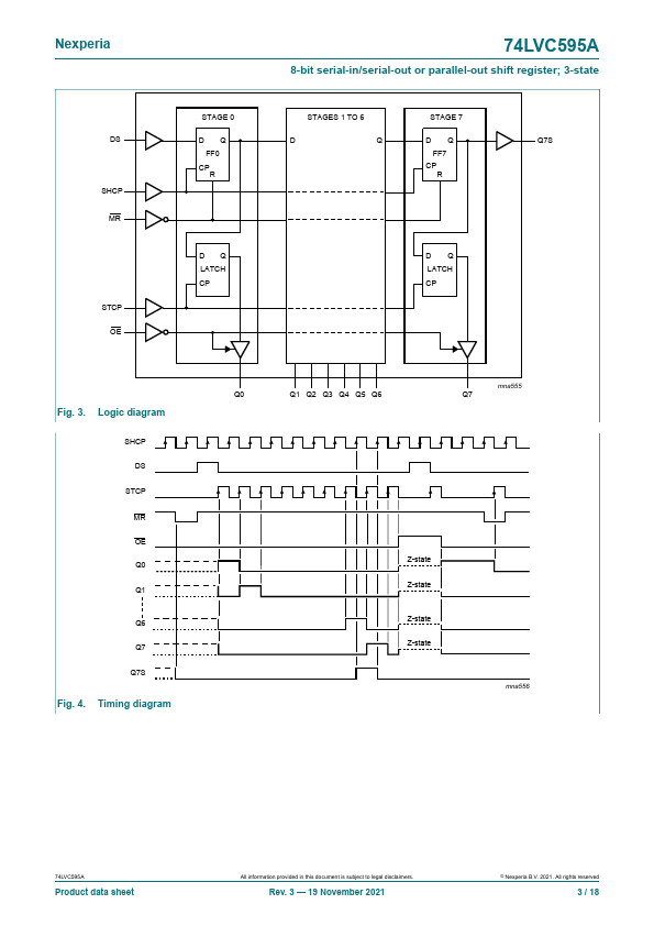
The 74LVC595A is an 8-bit serial-in/serial or parallel-out shift register with a storage register and 3-state outputs. Both the shift and storage register have separate clocks. The device features a serial input (DS) and a serial output (Q7S) to enable cascading and an asynchronous reset MR input. A LOW on MR will reset the shift register. Data is shifted on the LOW-to-HIGH transitions of the SHCP input. The data in the shift register is transferred to the storage register on a LOW-to-HIGH transition of the STCP input. If both clocks are connected together, the shift register will always be one clock pulse ahead of the storage register.
 74LVC595A Datasheet